It is divided into two stages. One is offline preparation. Second, online debugging. Each PCB factory also differs in specifIC details according to its SMT mounter model and management mode. Let me take our company's process as an example
The offline preparations are as follows:
First sort out the customer's information. Programming needs to be done on the computer, so it must be electronic. Generally in excel format

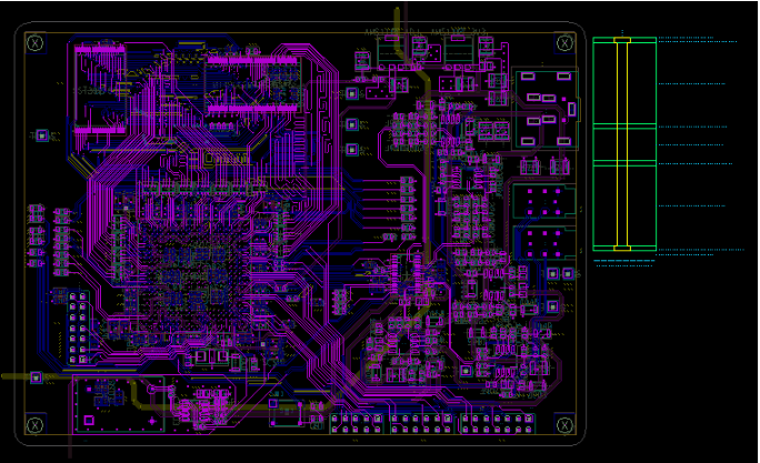
2. Extraction of coordinates. There are three situations: (1) If the customer sends the coordinates of the exported Excel or txt document, you can directly use the programming software to merge the coordinates with the BOM allocation you have sorted out.
(2). If the customer sends a PCB file, it is necessary to export the coordinates by itself. Generally, you can export the coordinates in excel format using protel99sse or PADS2007.
(3). The customer only provided a BOM allocation order, but could not provide coordinates. In this case, a scanner is needed. The scanned points are saved in CAD format, and then the coordinates and BOM allocation order are combined
3. After the BOM allocation sheet and coordinates are combined, check whether there are omissions or relocations. If yes, the Engineering Department needs to contact the customer for confirmation, and then save them in the format required by the machine.
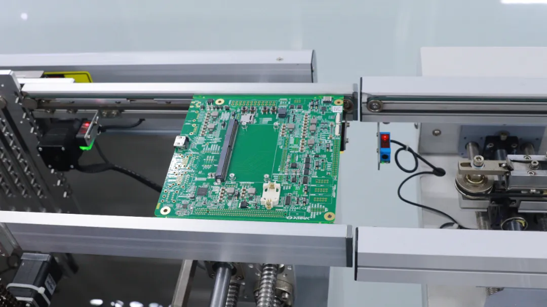
SMT patch
In these three steps, offline programming of SMT mounter is basically completed.
Online debugging:
1. Import the programmed program into the machine
2. Find the origin and make a MARK
3. Gradually correct the tag coordinates.
4. Optimize the saving program and check the component direction and data again
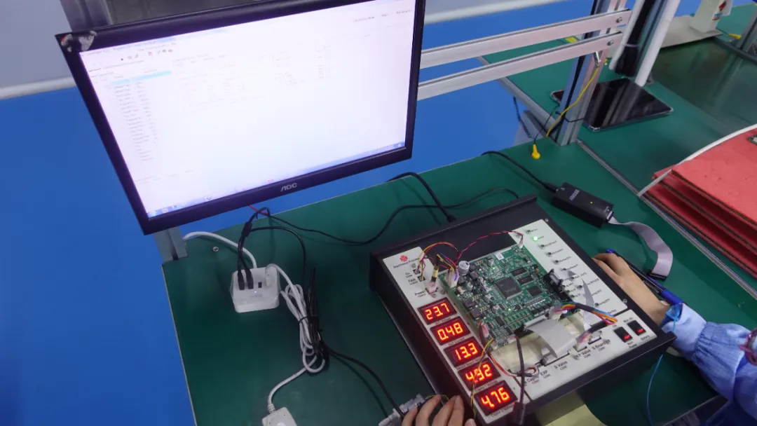
5. Start up and confirm the first article
What brand of model programming nothing more than these. I hope it will help you
Generally, it can be divided into two stages: offline preparation. Second, online debugging.
Each factory has different details according to its SMT mounter model and management mode
Programming is mainly divided into the following five points:
1. Get the production BOM, and figure out what patches to stick at each placement
2. Measure the patch coordinates, and find out the X, Y axis coordinates and Z axis parameters of each patch position
3. Measure the parameters of the patch, and figure out the shape, size, height, etc. of each patch
4. Measure the parameters of the SMD PCB board, and figure out the shape, size, height, etc. of the board to be SMD
5. The feeding parameters, and the feeding coordinates and height of each material
The production of circuit board is very SIMple. The program is well programmed. The production is carried out according to the corresponding program and materials. Pay attention to the PCB process parameters
The above answers have been very detaiLED. The general meaning of SMT programming and production is like this. If you want to be careful, you have to look at what the SMT is. The programming details of each machine are different
According to your circuit board design file, input the position of each component on the circuit board corresponding to the circuit board in the SMT mounter, and at the same time, input which feeder each component is on the mounter. After inputting these, the machine will know where to get the materials and then paste the PCB components.
然后
联系
电话热线
13410863085Q Q

微信

- 邮箱


