鑫景福致力于满足“快速服务,零缺陷,辅助研发”PCBA订购单需求。


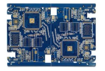
It is a necessary hard work for engineers to design circuits, but no matter how perfect the principle design is, if the performance is unreasonable, it will be greatly reduced, and even cannot work normally in serious cases. Based on the experience of the company's engineers, the following points for attention in PCB design are summarized.
No matter what PCB software is used, there is a general program for PCB design. It will save time and effort in order, so I will introduce it according to the production process.
SchematIC design is a preparatory work. It is often seen that beginners draw directly in order to save trouble. This will not pay off. For simple boards, if you are profICient in the process, you can skip it. But for beginners, we must follow the process. On the one hand, we can form good habits, and on the other hand, we can avoid mistakes for complex circuits.
When drawing schematic diagrams, pay attention to that each PCB file should be connected as a whole at the end of hierarchical design, which is also important for future work. Due to the difference of software, some software may appear to be connected but not actually connected (in terms of electrical performance). If you do not use the relevant detection tools to detect, in case of a problem, it will be late to find out when the board is ready. Therefore, we have repeatedly stressed the importance of doing things in order and hope to draw everyone's attention.
The schematic diagram is based on the design project. As long as the electrical connection is correct, there is nothing to say. Now let's focus on the problems in the specific procedure.
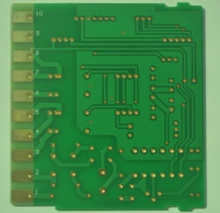
1. Make physical border
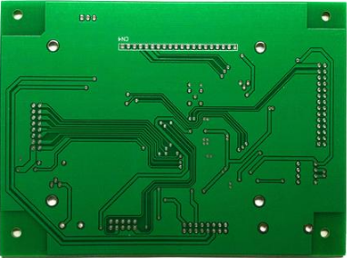
The closed physical frame is a basic platform for future component layout and routing, and also a constraint for automatic layout. Otherwise, the components coming from the schematic diagram will be at a loss. But you must pay attention to the accuracy here, otherwise you will have a lot of trouble in the future. Also, it is better to use arc at the corner, which can avoid sharp corner scratching workers on the one hand and reduce the stress effect on the other. In the past, one of my products was always broken in the process of transportation by a few machines. It would be better to use circular arc instead.
2. Introduction of components and networks
It should be easy to draw components and networks into the drawn border, but problems often occur here. Be careful to solve the problems one by one according to the prompted errors, otherwise it will take more effort later. The problems here are generally as follows:
The package form of the component cannot be found, the component network has problems, and there are unused components or pins. It is suggested that these problems can be solved quickly.
3. PCB layout
The layout and routing of components have a great impact on the life, stability and electromagnetic compatibility of products, which should be paid special attention to. Generally speaking, the following principles should be followed:
(1) Placement order
First place components at fixed positions related to the structure, such as power sockets, indicators, switches, connectors, etc. These components are locked with the lock function of the software after being placed, so that they will not be moved by mistake later. Then place special components and large components on the circuit, such as heating components, transformers, ICs, etc. Finally, place the SMAll device.
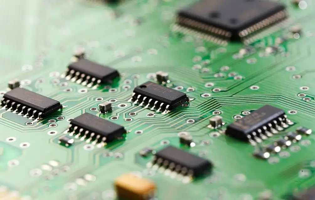
(2) Pay attention to heat dissipation
Special attention shall be paid to heat dissipation in PCB component layout. For high-power circuits, those heating elements such as power tubes and transformers should be placed as far away as possible to facilitate heat EMIssion. They should not be concentrated in one place, nor should high capacitors be too close to avoid premature aging of electrolyte.
To outline the circuit types in PCB design
11-10,2022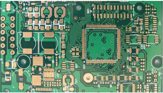

抖音二维码

Q Q二维码

微信二维码
点击
然后
联系
然后
联系
电话热线
13410863085Q Q

微信

- 邮箱