鑫景福致力于满足“快速服务,零缺陷,辅助研发”PCBA订购单需求。


Manufacturing method of copper clad laminate for PCB
PCB copper clad plate is the base material for manufacturing printed circuit board In addition to supporting various components, it can realize electrICal connection or electrical insulation between them In the manufacturing process, the PCB clad plate is used to DIP glass fiber cloth, glass fiber mat, paper and other epoxy resin reinforcement materials, phenolic resin and other adhesives, and dry it at an appropriate temperature to stage B to obtain the required PCB pre embedded material (Abbreviated as dipping material), then laminated with copper foil according to the process requirements, and heated and pressurized on the laminator to obtain the required PCB clad copper plate
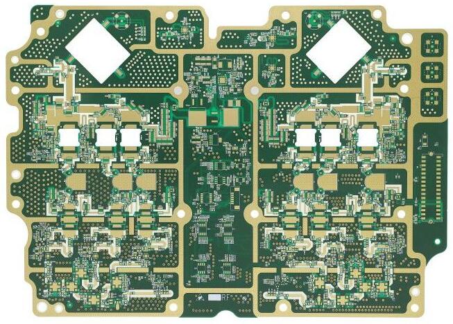
PCB board

1. classification of PCB board copper clad laminate PCB board copper clad laminate consists of three parts: copper foil, reinforcement materials and adhesive Plates are usually classified according to reinforcement grade and adhesive grade or plate characteristics
1. According to the classification of reinforcement materials, commonly used reinforcement materials PCB boards are aluminum free (aluminum metal oxide content not exceeding 0.5%) glass fiber products (such as glass cloth, glass mat) or paper (such as wood pulp paper, bleached wood pulp paper, lint paper) Therefore, PCB CCL can be divided into two types: glass cloth base and paper base
2. According to the type of adhesives, the adhesives used in PCB foil clad laminate are mainly phenolic resin, epoxy resin, polyester fiber, polyimide, polytetrafluoroethylene resin, etc Therefore, PCB foil clad laminate is also divided into phenolic resin Type, epoxy resin type, polyester type, polyimide type, PTFE type PCB laminate
3. According to the characteristics and uses of the base materials, and according to the burning degree of the base materials in the flame and after leaving the ignition source, they can be divided into universal type and self extinguishing type; According to the bending degree of the substrate, it can be divided into rigid and flexible PCB laminates; According to the operating temperature and environmental conditions of the substrate, it can be divided into heat resistant, radiation resistant, high-frequency PCB, foil clad, etc In addition, there are also foil clad laminates for special occasions of PCB boards, such as prefabricated inner laminate and metal based laminate, which can be divided into copper foil, nickel foil, silver foil and aluminum foil, Beryllium copper foil clad laminate
4. The commonly used PCB GB4721-1984 specifies the model of the foil clad laminate PCB CCL is usually composed of five English letters: the letter C represents CCL, and the second and third letters represent the base material Selected adhesive resin For example, PE represents phenolic; EP refers to epoxy resin; UP represents unsaturated polyester; SI refers to silica gel; TF refers to polytetrafluoroethylene; PI refers to polyimide The fourth and fifth letters represent the reinforcement data selected for the base material For example, CP refers to cellulose fiber paper; GC refers to alkali free glass fiber cloth; GM refers to alkali free glass fiber felt For example, if the inner core PCB laminate of the master data is reinforced with fiber paper and cellulose, and the alkali free glass cloth is pasted on both sides, the two digits on the right side of the horizontal line in the model can be added after the CP to represent the product numbers of the same type and different effectiveness For example, the number of copper clad phenolic paper laminates is O1~20, and the number of copper clad epoxy paper laminates is 21~30; The number of copper clad epoxy glass cloth laminates is 31~40. The letter F indicates that the PCB is self extinguishing
2. Manufacturing method of copper clad laminate PCB manufacturing of copper clad laminate PCB mainly includes three steps of resin solution preparation, reinforcement material immersion and compression molding
1. The main raw materials for manufacturing CCL PCB The main raw materials for manufacturing CCL are resin, paper, glass cloth, and copper foil
(1) the resin used for the copper clad laminates of The resin PCBs include phenolic, epoxy resins, polyester fiber, polyimide, etc Among them, the amount of phenolic resin and epoxy resin Phenolic resin is a kind of resin formed by condensation of phenol and aldehyde in acidic or alkaline medium Among them, the resin polycondensated with phenol and formaldehyde in alkaline medium is the main raw material for paper making In order to obtain a variety of circuit boards with excellent performance, it is usually necessary to modify the phenolic resin with various pipes and strictly control the content of free phenol and volatile matter of the resin to ensure that the board is in the thermal shock state No layering, no foam Epoxy resin is the main raw material of glass cloth. It has excellent bonding performance and electrical and physical properties The more commonly used types are E-20, E-44, E-51 and self extinguishing E-20 and E-25. In order to improve the transparency of the substrate, and to check the pattern defects in the production of printed boards, the epoxy resin color is required to be light
(2) Impregnated paper commonly used Impregnated paper includes cotton lint paper, wood pulp paper and bleached wood pulp paper Cotton lint paper is made of short fiber cotton fiber, which is characterized by better resin permeability, better board stamping and power efficiency Wood pulp paper is mainly made of wood fiber. Its price is usually lower than that of cotton linter paper, and it has higher mechanical strength Bleached wood pulp paper can improve the appearance of paperboard In order to improve the performance of the board, thickness deviation and weight, it is necessary to ensure the breaking strength and water absorption of impregnated paper
(3) Alkali free glass cloth For special high-frequency applications, quartz glass cloth can be used For the Alkali content of Alkali free glass cloth (expressed as Na20), it shall not exceed 1% according to the IEC standard, 0.8% according to the JIS standard R3413-1978, and 0.5% according to the former Soviet Union's TOCT5937-68 standard The standard JC-170-80 of the Ministry of Construction of China shall not exceed 0.5% In order to meet the general needs, thin multilayer printed boards and foreign glass cloth model PCB laminates have been serialized Its thickness ranges from 0.025 to 0.234 mm Glass cloth with special requirements shall be treated through the coupling In order to improve the processing efficiency of epoxy glass cloth PCB foil composite board and reduce the cost of the board, non woven glass fiber (also known as glass mat) has been developed in recent years
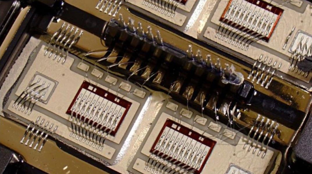
(4) The foil of copper foil PCB can be made of copper, nickel, aluminum and other metal foils However, considering the conductivity, solderability, elongation, adhesion to the substrate and the price of metal foil, copper foil is applicable except for special purposes Copper foil can be divided into rolLED copper foil and electrolytic copper foil Rolled copper foil is mainly used for Flexible printed circuits and other special purposes Electrolytic copper foil is widely used in the production of foil clad PCB The purity of copper shall not be lower than 99.8% according to IEC-249-34 and Chinese standards At present, the copper foil thickness of doMEStic printed boards is mostly 35um, and the transition product is 50um copper foil It is used to manufacture high-precision hole metallized double-sided or multilayer boards. It is expected to use copper foil with thickness less than 35um, such as 18um, 9um and 5um Some Multilayer boards use thicker copper foil, such as 70um A layer of copper oxide or cuprous oxide is formed on the surface of copper foil, Which improves the bonding strength between the copper foil and the abstract due to the effect of polarity) or roughened copper foil (a roughening layer is formed on the surface of the copper foil by electrical methods.) In order to avoid copper oxide powder falling off and moving to the substrate, the surface treatment method of copper foil is also constantly improved For example, TW copper foil is coated with a thin layer of zinc on the rough surface of the copper foil, and the surface of the copper foil is gray at this time; TC type copper foil is coated with a thin layer of copper zinc alloy on the rough surface of copper foil When the surface of copper foil is gold After special treatment, the resistance to heat and discoloration, oxidation resistance and cyanide resistance of copper foil in PCB manufacturing are improved accordingly The copper foil surface shall be smooth without obvious wrinkles, oxidation points, scratches, pits, pits and stains Porosity of 305g copper foil/m2 and above requirements no more than 8 penetration points in an area of 300ram * 300mm; The total point area of copper foil in an area of 0.5m2 does not exceed the area of a circle with a diameter of 0. 125 mm Porosity and pore diameter/m2 of copper foil below 305g shall be negotiated by both parties Before putting the copper foil into use, if necessary, take samples for pressing test The compression test shows its peel strength and general surface quality
Writing Skills of PCB Design Rule Checker
11-07,2022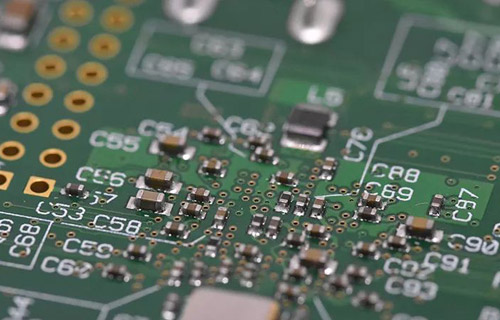

抖音二维码

Q Q二维码

微信二维码
点击
然后
联系
然后
联系
电话热线
13410863085Q Q

微信

- 邮箱