Reduce automobile PCB defects and avoid PCB CAM
The Automotive electronics MARKet is the third largest field of printed circuit board applICations after computers and communications With the gradual evolution and development of automobile from traditional mechanical products to intelligent, information-based, mechatronic high-tech products, electronic technology has been widely used in automobiles. Whether it is engine system, chassis system, safety system, information system, and interior environment system all use electronic products without exception The automobile market has obviously become another highlight of the electronic consumer market The development of automotive electronics naturally promotes automotive PCBs
In today's key PCB applications, Automotive PCB plays an important role. However, due to the special working environment,
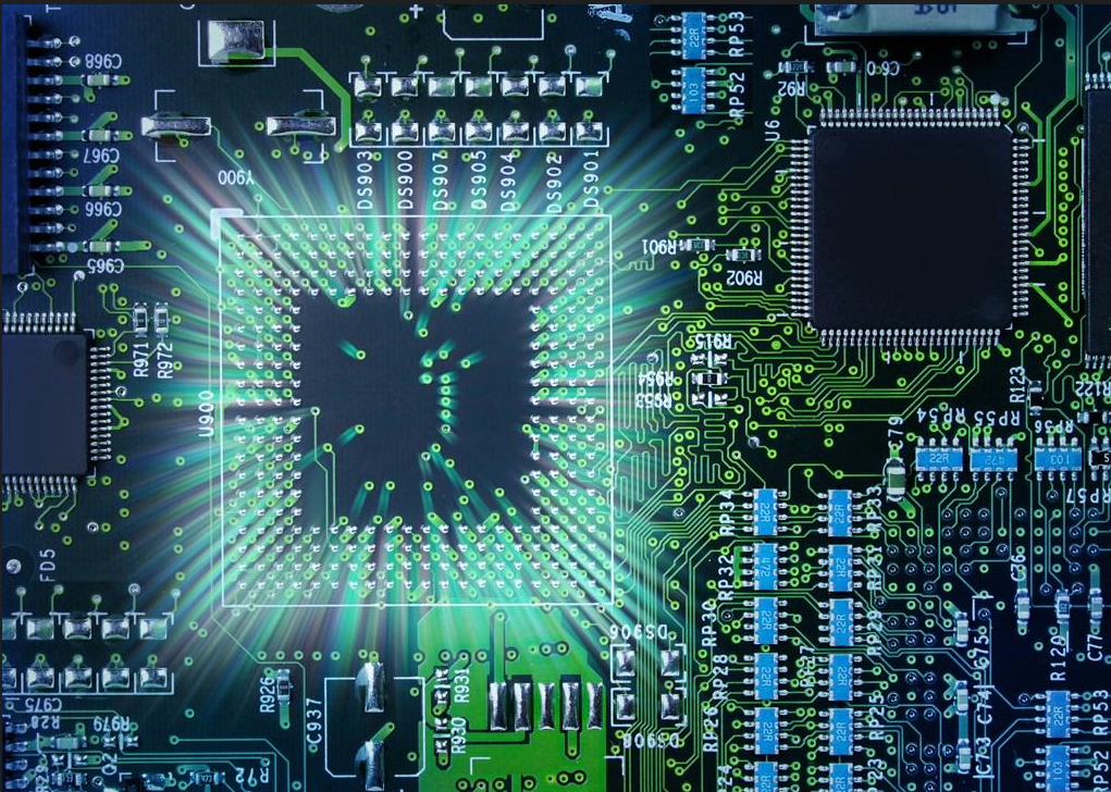
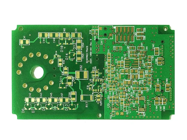
Circuit board

The safety and high current requirements of automobiles have higher requirements on the reliability and environmental adaptability of printed circuit boards, and involve a wide range of PCB technology types This is a problem for PCB companies The challenge is for manufacturers who want to develop the automobile PCB market. They need to have more understanding and analysis of this new market
Automotive PCB emphasizes high reliability and low DPPM. So, does our company have accumulated technology and experience in high reliability manufacturing? Is it consistent with the future product development direction? In terms of process control, can it be done well according to the requirements of TS16949? Is low DPPM achieved? All these need to be carefully evaluated. Just seeing this tempting cake and blindly entering it will hurt the enterprise itself.
The following are some special practices of some representative companies specializing in the production of automotive PCB in the testing process, for reference by most PCB colleagues:
The second test method
Some PCB manufacturers use the "second test method" to improve the speed of finding defective circuit boards after the first high-voltage electrical breakdown.
Testing system for no risk of broken boards
More and more printed circuit board manufacturers have instalLED "good board marking system" and "bad board error proofing box" on the optical board testing machine, effectively avoiding man-made leakage. A good board marking system marks qualified boards for the testing machine, which can effectively prevent test boards or defective boards from flowing into the hands of customers. Error proofing box of defective board refers to the signal that the test system outputs the box to open when the board is tested to be qualified during the test; On the contrary, when testing a bad board, the box will close to allow the operator to correctly place the board under test.
When you create Gerber archives for PCB design, it is sometiMES difficult to accurately reflect the products you want to manufacture. However, Advanced Circuits provides some useful tips that can help you reduce the possibility that PCB orders are shelved, thereby reducing turnaround time and obtaining the required boards. Some of the most common mistakes designers make are neglecting the hole diameter list, borehole file, borehole list or its Gerber file. Sometimes, the design itself may not be complete or meet manufacturing requirements.
SIMplify PCB design process by using advanced circuits
If you use the FreeDFM system provided by Advanced Circuits, it will simplify the design and submission process. With integration, you can view any potential DFM issues so that they can be properly resubmitted using the same interface. In this way, the design submission and manufacturing process are completed by a professional company, so that we can know whether the printed circuit board meets the requirements.
然后
联系
电话热线
13410863085Q Q

微信

- 邮箱


