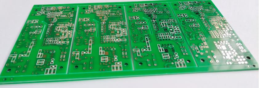
PCB Factory: How many do you know about the PCB jargon test?
PCB manufacturers, PCB designers and PCBA manufacturers explain to you that PCB manufacturers: how many PCB jargon tests do you know?
"The king of heaven covers the earth!"
"The pagoda controls the river demon!"
"Huh? Huh?"
"Nobody has a home when he speaks at noon!"
Full of jargon and argot
It is diffICult to understand at first
But careful taste can also help
Identify the identity, background and lifestyle of the role
This is the legendary "jargon"
There are many such "jargon" in all walks of life
In the circuit board industry
There are also many "jargon" widely spread
The SMAll editor of circuit board CAMe to test everyone
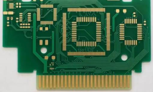
[Golden Finger]
Gold Finger, or Edge Connector, is designed to conduct conductive interconnection by pressing contact with the connection between the connector spring.
Gold was chosen because of its superior conductivity and oxidation resistance. The golden finger is the row of golden objects in the memory module or video card version of your computer.

Hard Gold
The purpose of electroplating is basically to plate "gold" on the copper skin of the circuit board. However, if "gold" and "copper" are in direct contact, there will be a physical reaction of electron migration and diffusion (potential difference relationship).
Therefore, a layer of "nickel" must be plated first as a barrier layer, and then gold must be plated on the nickel. Therefore, the actual name of the so-calLED electroplated gold should be "electroplated nickel gold".
Soft Gold
Electroplating soft gold is to deposit nickel and gold on the circuit board by electroplating, and its thickness control is flexible. Generally, it is used for making aluminum wire on COB (Chip On Board) or the contact surface of mobile phone keys. Most of the electroplating gold used for gold finger or other adapter cards or memory is hard gold, because it must be wear-resistant.
[Through hole]
The copper foil circuit between conductive patterns in different layers of the circuit board is conducted or connected by this kind of hole, but it is not allowed to insert the copper plated holes of component legs or other reinforcement materials. Printed circuit board (PCB) is formed by stacking many copper foil layers. The reason why copper foil layers cannot communicate with each other is that each layer of copper foil is paved with an insulating layer, so they need to rely on via for signal link, so they have the Chinese name of via.
Blind hole
The outermost circuit of the circuit board is connected to the adjacent inner layer with electroplated holes. Because the opposite side cannot be seen, it is called "blind hole". In order to increase the space utilization of PCB circuit layers, the "blind hole" process came into being. The blind hole is located on the top layer and bottom layer of the circuit board, and has a certain depth. It is used to connect the surface layer circuit with the lower inner layer circuit. The depth of the hole generally has a specified ratio (aperture).
[Buried hole]
Buried hole refers to the connection between any circuit layers in a Printed Circuit Board (PCB), but it is not conductive to the outer layer, that is, there is no conductive hole extending to the surface of the PCB. This manufacturing process cannot be achieved by drilling holes after bonding circuit boards. Drilling operations must be carried out at the time of individual circuit layers. First, local bonding of the inner layer is followed by electroplating, and finally, all bonding is carried out. PCB manufacturers, PCB designers and PCBA manufacturers explain to you that PCB manufacturers: how many PCB jargon tests do you know?
然后
联系
电话热线
13410863085Q Q

微信

- 邮箱


