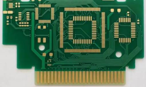
Is the gold finger on the circuit board of the circuit board factory really gold?
The Circuit board manufacturer, circuit board designer and PCBA manufacturer explain to you whether the golden finger on the circuit board of the Circuit board factory is really gold?
On the computer memory module and video card, we can see a row of golden conductive contacts, whICh are calLED "golden fingers". The Gold Finger (or Edge Connector) in the PCB design and manufacturing industry uses the connector connector as the outlet of the board's external connection network. Next, I will discuss the handling method and some details of the golden finger in PCB with the SMAll editor of the circuit board factory.
Surface treatment method of gold finger PCB
Nickel gold plating: the thickness can reach 3-50u ". Because of its superior conductivity, oxidation resistance and wear resistance, it is widely used on gold finger PCBs that require frequent plugging or mechanical friction. However, because of the high cost of gold plating, it is only used for local gold plating treatment such as gold finger.
2. Gold deposition: the thickness is generally 1u ", up to 3u". Because of its superior conductivity, flatness and solderability, it is widely used in high-precision PCB boards designed by key position, binding IC, BGA, etc. For gold finger PCB with low wear resistance requirements, the whole board gold deposition process can also be selected. The cost of the gold deposition process is much lower than that of the electric gold process. The color of the gilding process is golden yellow.
Gold finger detail processing in PCB of circuit board factory

1) In order to increase the wear resistance of gold finger, gold finger usually needs to be plated with hard gold.
2) The golden finger needs to be chamfered, usually 45 °, and other angles such as 20 °, 30 °, etc. If there is no chamfer in the design, there is a problem; The 45 ° chamfer in PCB is shown in the following figure:
3) The golden finger needs to be welded as a whole to open the window, and the PIN does not need to open the steel mesh;
4) The minimum distance between tin and silver pads and the tip of the finger is 14mil; It is recommended that the pad should be more than 1mm from the finger position, including via pad;
5) The surface of gold finger shall not be covered with copper;
6) All layers of the inner layer of the golden finger need to be copper chipped, usually 3mm wide; Can do half finger copper cutting and whole finger copper cutting.
Is the "gold" in the finger of a circuit board factory gold?
First, let's understand two concepts: soft gold and hard gold. Soft gold, generally soft gold. Hard gold, generally a compound of hard gold.
The main function of golden finger is connection, so it must have good conductivity, wear resistance, oxidation resistance and corrosion resistance.
Because pure gold (gold) is relatively soft, gold finger generally does not use gold, but only plating a layer of "hard gold (gold compound)" on it, which can not only obtain good conductivity of Jinliang, but also make it have wear resistance and oxidation resistance.
Have you ever used "soft gold" for PCB? The answer is of course useful, such as the contact surface of some mobile phone keys, and the aluminum wire on the COB (Chip On Board). Soft gold is generally used to precipitate nickel gold on the circuit board by electroplating, and its thickness control is flexible. The circuit board manufacturer, circuit board designer and PCBA manufacturer explain to you whether the golden finger on the circuit board of the circuit board factory is really gold?.
然后
联系
电话热线
13410863085Q Q

微信

- 邮箱


