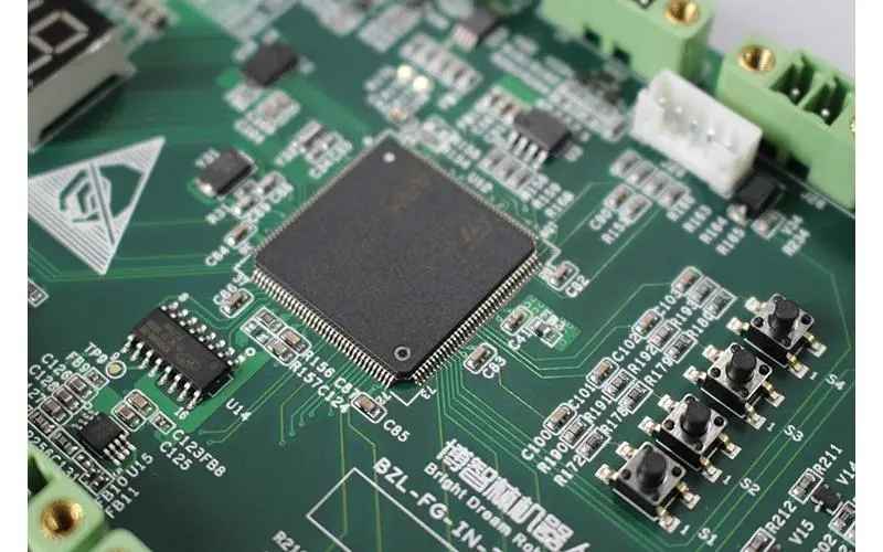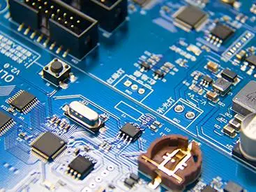
circuit boards are found in almost every electronIC device you use, and while they're common, that doesn't mean they're SIMple. printed circuit boards are a complex business, and assembling them correctly requires the right tools, the right parts, and the right know-how. Trusting a professional to perform the assembly means ensuring that throughout the process, quality control measures will be followed and tests will be performed so that you can rest assured of knowing when you receive the PCB and that it will run as needed. But what is the process of PCBA assembly? Do you need to simply let the company know what you need, or do you need to submit each part?

Select turnkey printed circuit board assembly is an excellent solution for any business. Using this option, our professionals will gather all the necessary parts and components and assemble the PCB. This PCBA production solution is cost effective and helps save time because we will ensure we have everything we need to build correctly.
A kit of printed circuit board components is a perfect choice for someone who knows exactly what PCB they want, but may not have the time or equipment to assemble it. You can buy all the components and parts you want and need from PCBA manufacturers and use them. This can help you better control production costs and understand what to expect from the finished printed circuit board.
Perhaps you know some components to use in your PCB, but still need some parts to complete your PCB electromechanical assembly -- this is where combined-PCB assembly coMES in. You supply us with the parts and components you have and we will supply whatever you still need and put it together professionally. This option still allows you to have some control over production costs, as well as control over your most important components, combined with the ease and time-saving ability of PCBA manufacturers to get the job done.
1, according to the type of substrate:
(1) Flexible PCB board: printed circuit board made of flexible substrate, which has the advantage of being able to bend and easy to assemble electrical components. FPC has been widely used in aviation, military, mobile communications, laptop computers, computer peripherals, PDAs, digital CAMeras and other fields or products.
(2) Rigid PCB board: made of paper base or glass cloth, preimpregnated phenolic or epoxy resin, the surface adhered to one or both sides of the copper foil, and then laminated curing; It is rigid, does not bend easily, and can be attached to electronIC components to provide a degree of support.
(3) soft and hard combined PCB board (rigid flexure combined board) : by the rigid board and flexible board laminated together. The advantage is that it can not only provide the support function of rigid printing plate, but also have the bending characteristics of flexible plate, which can meet the needs of 3D assembly.
2, according to the number of layers:
(1)Single panel: On the most basic printed circuit board, the parts are concentrated on one side and the wires are concentrated on the other side. Because the wires appear on only one side, the printed circuit board is calLED a single panel.
(2) Dual panel: each side of the circuit board is wired. In order to connect the wires on both sides, a proper circuit connection must be made between the two sides, which is called a pilot hole and is used on more complex circuits than a single panel.
(3) Multilayer board: in order to increase the area of wiring, more single-sided or double-sided wiring board is used, and the insulation layer is placed after adhesion on each layer; The number of layers on the board represents several independent wiring layers, usually an even number, and contains the outermost two layers.
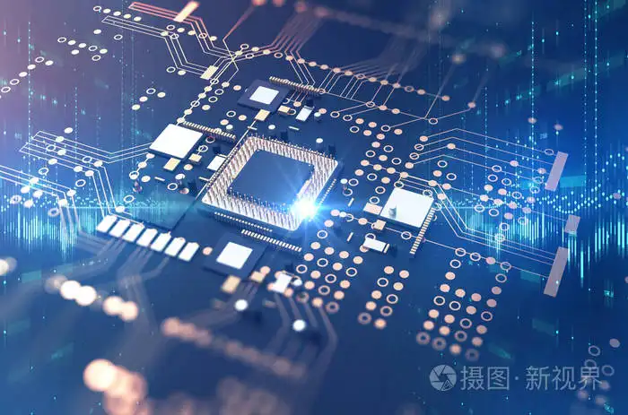
Components of pcb circuit board:
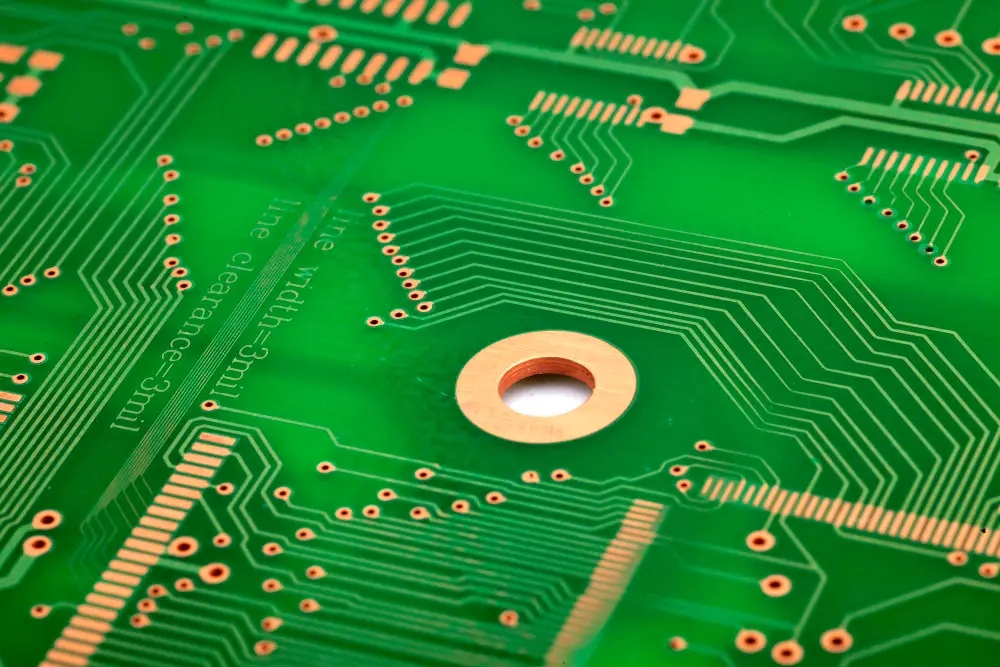
Lines and patterns: Lines are used as a transmission tool between manuscripts. In the design, a large copper surface will be designed as the grounding and supply layer. The lines and drawings are made simultaneously.
Dielectric layer: used to maintain the insulation between the line and the layer, commonly known as the substrate.
Through-hole/Through-hole: The through-hole allows two or more layers of circuits to pass each other. The larger through-hole is used as part of the plug-in, and the non-through-hole (nPTH) is usually used as the positioning of the surface patch. It is used for fixing screws during assembly.
Solder resistance/solder resistance: not all copper surfaces require the tin part, so the non-tin area will be printed with a layer of material (usually epoxy) to isolate the copper surface from the tin and avoid short circuit between the wires that do not eat tin. According to different processes, it is divided into green oil, red oil and blue oil.
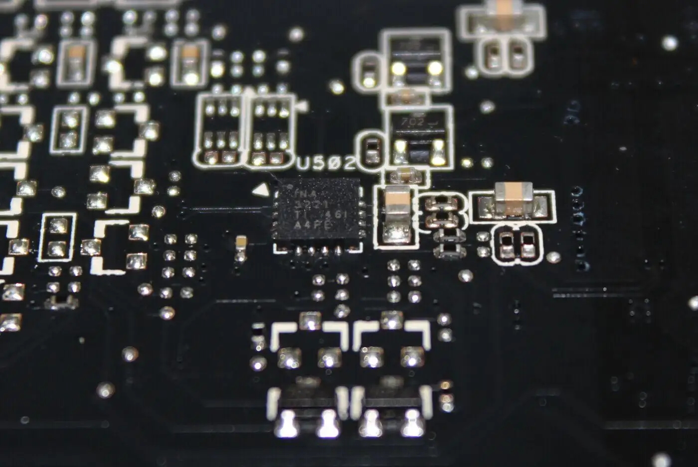
Legend/MARKing/Silk Screen: This is a non-essential component. The main function is to mark the name and position box of each part on the circuit board, so as to facilitate the maintenance and identification after assembly.
Surface treatment: Because the copper surface is easy to oxidize in the general environment, can not be on the tin (poor weldability), so it will protect the copper surface that needs to eat tin. Protection methods include spray Tin (HASL), chEMIcal gold (ENIG), chemical Silver (Immersion Silver), chemical Tin (Immersion Tin), organic solder protective agent (OSP), each method has advantages and disadvantages, collectively known as surface treatment.
For more information about the PCB assembly options available to us, please view our quotation sheet flow page, or contact us now.
然后
联系
电话热线
13410863085Q Q

微信

- 邮箱


