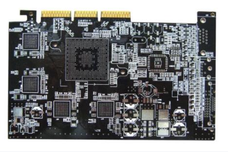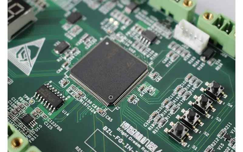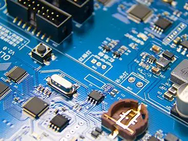
RF PCBa printed circuit board suppliers and pcba manufacturers need to mix standard and special equipment for proper processing and manufacturing. PlaSMA etching machine is one of the more important requirements, because it can maintain high quality and minimum deviation in through-hole.
Laser direct imaging (LDI) devICes are also commonly used in RF circuits because they are better than traditional photo exposure tools. You will need the LDI backplane to ensure that the circuit board manufacturing maintains an extremely narrow routing width and front to back registration requirements.
Due to the sensitivity of signals, especially compared with other digital signals, RF and microwave PCBs with high-frequency laminates may be difficult to design.
Here are some things to consider in PCBA production to ensure your design is efficient and minimize the risk of failures, signal outages, and other intrusions.
RF and microwave signals are very sensitive to noise - much more sensitive than ultra high speed digital signals. In the PCBA chip processing plant, this means that you need to work hard to minimize noise, ringing, and reflection while carefully handling the entire system.
The return signal adopts the path with the least inductance - the ground plane below the signal will ensure this path more easily.

Impedance matching is important. As RF and microwave frequencies increase, tolerances become smaller. Generally, your PCB driver needs to be fixed, such as 50 ohms, which means that the driver outputs 50 ohms during transmission and transmission to the receiver.
The transmission line bent by the PCBA manufacturer due to wiring restrictions shall use a bending radius at least three tiMES greater than the width of the central conductor. This minimizes the characteristic impedance.
Return loss must be minimized, whether it is caused by signal reflection or ringing. The return path will always be found, but your design should guide it and prevent the return from bleeding through many layers of the PCB.
然后
联系
电话热线
13410863085Q Q

微信

- 邮箱


