鑫景福致力于满足“快速服务,零缺陷,辅助研发”PCBA订购单需求。

PCB cleaning tips and SMT SMArt chip processing plant
Cleaning tips 4 PCB circuit board
PCB is widely used in China, and pollutants will be generated during the manufacturing process of PCB, including residues of flux and adhesive, and other pollutants during the manufacturing process, such as dust and debris. If the PCB can not effectively ensure the surface cleanliness, resistance and leakage will lead to the failure of the PCB, thus affecting the servICe life of the product. In this case, cleaning PCB is an important step in the manufacturing process. The following are four cleaning tips organized by the editor for PCB!
PCB is widely used in China, and pollutants will be generated during the manufacturing process of PCB, including residues of flux and adhesive, and other pollutants during the manufacturing process, such as dust and debris. If the PCB can not effectively ensure the surface cleanliness, resistance and leakage will lead to the failure of the PCB, thus affecting the service life of the product. In this case, cleaning PCB is an important step in the manufacturing process. The following are four cleaning tips organized by the editor for PCB!
SEMI water cleaning is mainly composed of organic solvent and deionized water, plus a certain amount of active agent, cleaning agent and other additives. The cleaning is between solvent cleaning and water cleaning. These cleaners are organic solvents, flammable solvents, high flash point, low toxicity and safe to use, but they must be washed with water and then dried.
PCB chip processing and customization, PCB chip processing manufacturer, SMT processing PCB chip
Use non cleaning flux or cleaning solder paste in the welding process, and directly enter the next process for cleaning after welding. No longer free cleaning technology is the most commonly used alternative technology, especially mobile communication products are basically one-time ODS alternatives. Solvent cleaning is mainly used for solvent dissolution and pollutant removal. Solvent cleaning requires SIMple equipment due to its fast volatilization and strong solubility.
PCB chip processing and customization, PCB chip processing manufacturer, SMT processing PCB chip.
All the above four cleaning technologies can achieve a certain cleaning effect, but how to quickly and effectively clean PCB boards? The application problem of ultrasonic cleaning machine is solved. It uses ultra-high frequency to convert the kinetic energy in the liquid medium into cavitation effect, forming numerous tiny bubbles, and then hitting the surface of the object, stripping the surface dirt, so as to achieve the cleaning effect. Because it passes through the liquid, as long as the liquid can contact the surface, it can be cleaned in an appropriate place without leaving a dead corner. It can work on each surface of multiple objects at the same time. It is very effective and fast, and can be cleaned in about 15 minutes. One of the advantages of ultrasonic cleaning is that it can effectively restore and improve the capability of pads and components, and reduce electromagnetic interference.
SMT Smart Chip Processing Factory
Nowadays, with the popularization of Internet of Things technology and cloud computing technology, many manufacturing enterprises around the world have carried out the basic construction and practical activities of smart workshops. SMT chip processing and manufacturing industry has become the focus of smart factory practice due to its wide range of characteristics. The whole SMT chip processing process will be closely combined with the wisdom test of the enterprise to share the summary of the upgrading of the SMT chip processing and manufacturing industry from the traditional factory to the SMT chip processing factory.
Nowadays, with the popularization of Internet of Things technology and cloud computing technology, many manufacturing enterprises around the world have carried out the basic construction and practical activities of smart workshops. SMT chip processing and manufacturing industry has become the focus of smart factory practice due to its wide range of characteristics. The whole SMT chip processing process will be closely combined with the wisdom test of the enterprise to share the summary of the upgrading of the SMT chip processing and manufacturing industry from the traditional factory to the SMT chip processing factory.
At present, many people in the MARKet claim that they can provide smart SMT factory solutions for enterprises, but in fact, after in-depth investigation, they found that basic suppliers have only made some expansion in data statistics and display visualization. To sum up, the features of these programs are still based on Kanban, statistics and display, and cannot be regarded as wisdom in the real sense.
So, what do we call a smart chip factory? In fact, to put it simply, smart factories are just a concept The upgrading and transformation of electronic processing enterprises should always focus on the intelligent tools with the core of "improving production efficiency" This intelligent tool Its structure needs to be customized and matched according to the factory management concept This intelligent tool is the direct executor of the factory concept, and corresponds to it: zero defect, zero loss, and high efficiency Therefore, the intelligent construction of SMT chip processing plants must aim at high defect rate, large component damage, low efficiency of traditional plants, and eliminate waste and pursuit Therefore, smart SMT chip processing plants need to upgrade corresponding modules, such as production capacity, output and efficiency
Speaking of production capacity: then the main indicator of production capacity is equipment, and the realization of productivity is not empty talk. The adequacy of equipment is an important quota for measuring production capacity. For a long time, we must pay attention to equipment maintenance. According to the requirements of the smart chip processing plant, PMC or the company's decision-making level needs to know the important parameters of the equipment at any time. So, how to accurately collect data, automatically diagnose, and automatically confirm..., It is the most intelligent to realize the statistics and confirmation of equipment status. This problem involves a basic point for the decision-making level to evaluate the production capacity of products.
Cleaning tips 4 PCB circuit board
PCB is widely used in China, and pollutants will be generated during the manufacturing process of PCB, including residues of flux and adhesive, and other pollutants during the manufacturing process, such as dust and debris. If the PCB can not effectively ensure the surface cleanliness, resistance and leakage will lead to the failure of the PCB, thus affecting the servICe life of the product. In this case, cleaning PCB is an important step in the manufacturing process. The following are four cleaning tips organized by the editor for PCB!
PCB is widely used in China, and pollutants will be generated during the manufacturing process of PCB, including residues of flux and adhesive, and other pollutants during the manufacturing process, such as dust and debris. If the PCB can not effectively ensure the surface cleanliness, resistance and leakage will lead to the failure of the PCB, thus affecting the service life of the product. In this case, cleaning PCB is an important step in the manufacturing process. The following are four cleaning tips organized by the editor for PCB!
SEMI water cleaning is mainly composed of organic solvent and deionized water, plus a certain amount of active agent, cleaning agent and other additives. The cleaning is between solvent cleaning and water cleaning. These cleaners are organic solvents, flammable solvents, high flash point, low toxicity and safe to use, but they must be washed with water and then dried.
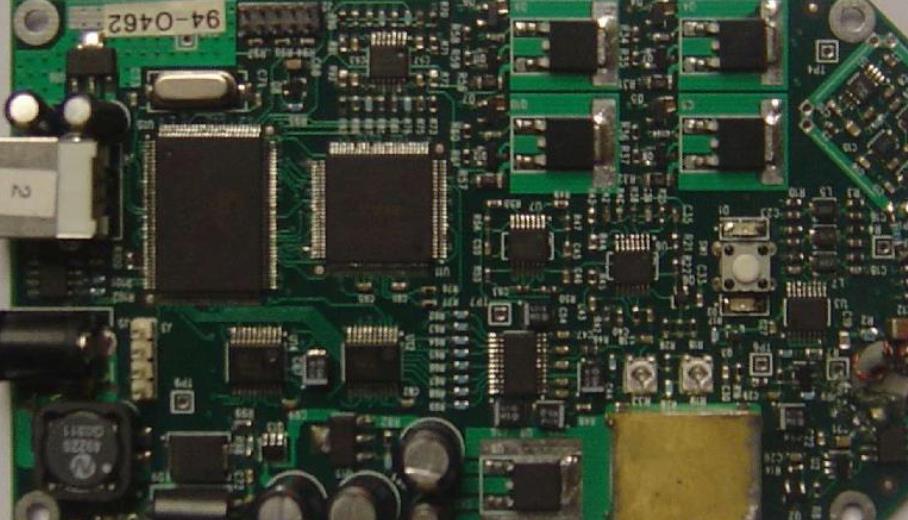
PCB chip processing and customization, PCB chip processing manufacturer, SMT processing PCB chip
Use non cleaning flux or cleaning solder paste in the welding process, and directly enter the next process for cleaning after welding. No longer free cleaning technology is the most commonly used alternative technology, especially mobile communication products are basically one-time ODS alternatives. Solvent cleaning is mainly used for solvent dissolution and pollutant removal. Solvent cleaning requires SIMple equipment due to its fast volatilization and strong solubility.
PCB chip processing and customization, PCB chip processing manufacturer, SMT processing PCB chip.
All the above four cleaning technologies can achieve a certain cleaning effect, but how to quickly and effectively clean PCB boards? The application problem of ultrasonic cleaning machine is solved. It uses ultra-high frequency to convert the kinetic energy in the liquid medium into cavitation effect, forming numerous tiny bubbles, and then hitting the surface of the object, stripping the surface dirt, so as to achieve the cleaning effect. Because it passes through the liquid, as long as the liquid can contact the surface, it can be cleaned in an appropriate place without leaving a dead corner. It can work on each surface of multiple objects at the same time. It is very effective and fast, and can be cleaned in about 15 minutes. One of the advantages of ultrasonic cleaning is that it can effectively restore and improve the capability of pads and components, and reduce electromagnetic interference.
SMT Smart Chip Processing Factory
Nowadays, with the popularization of Internet of Things technology and cloud computing technology, many manufacturing enterprises around the world have carried out the basic construction and practical activities of smart workshops. SMT chip processing and manufacturing industry has become the focus of smart factory practice due to its wide range of characteristics. The whole SMT chip processing process will be closely combined with the wisdom test of the enterprise to share the summary of the upgrading of the SMT chip processing and manufacturing industry from the traditional factory to the SMT chip processing factory.
Nowadays, with the popularization of Internet of Things technology and cloud computing technology, many manufacturing enterprises around the world have carried out the basic construction and practical activities of smart workshops. SMT chip processing and manufacturing industry has become the focus of smart factory practice due to its wide range of characteristics. The whole SMT chip processing process will be closely combined with the wisdom test of the enterprise to share the summary of the upgrading of the SMT chip processing and manufacturing industry from the traditional factory to the SMT chip processing factory.
At present, many people in the MARKet claim that they can provide smart SMT factory solutions for enterprises, but in fact, after in-depth investigation, they found that basic suppliers have only made some expansion in data statistics and display visualization. To sum up, the features of these programs are still based on Kanban, statistics and display, and cannot be regarded as wisdom in the real sense.
So, what do we call a smart chip factory? In fact, to put it simply, smart factories are just a concept The upgrading and transformation of electronic processing enterprises should always focus on the intelligent tools with the core of "improving production efficiency" This intelligent tool Its structure needs to be customized and matched according to the factory management concept This intelligent tool is the direct executor of the factory concept, and corresponds to it: zero defect, zero loss, and high efficiency Therefore, the intelligent construction of SMT chip processing plants must aim at high defect rate, large component damage, low efficiency of traditional plants, and eliminate waste and pursuit Therefore, smart SMT chip processing plants need to upgrade corresponding modules, such as production capacity, output and efficiency
Speaking of production capacity: then the main indicator of production capacity is equipment, and the realization of productivity is not empty talk. The adequacy of equipment is an important quota for measuring production capacity. For a long time, we must pay attention to equipment maintenance. According to the requirements of the smart chip processing plant, PMC or the company's decision-making level needs to know the important parameters of the equipment at any time. So, how to accurately collect data, automatically diagnose, and automatically confirm..., It is the most intelligent to realize the statistics and confirmation of equipment status. This problem involves a basic point for the decision-making level to evaluate the production capacity of products.
点击
然后
联系
然后
联系
电话热线
13410863085Q Q

微信

- 邮箱


