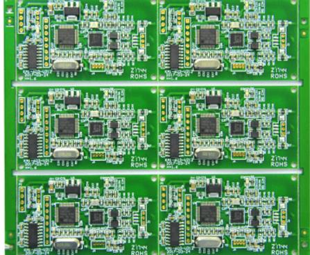
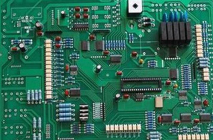
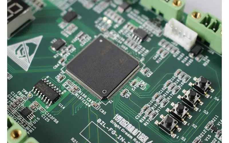
鑫景福致力于满足“快速服务,零缺陷,辅助研发”PCBA订购单需求。

chip mounter development and PCB electrostatIC protection
Development direction: mounting machine
With the rapid development of Surface Mount Technology, not only the size of electronIC components is getting SMAller and smaller, but also the assembly density of patches is getting higher and higher, and new packaging forms are constantly introduced to better apply high-density and difficult patches. With the development of processing and assembly technology, the SMT machine is gradually developing towards a high level, multi-function, modular and intelligent direction.
1. High speed
1. "Flight alignment" technology. Flight alignment technology directly installs the CCD image sensor on the placement head, moves and fixes the CCD image sensor and picks up the equipment at the same time, and then performs optical centering on the components when moving to the placement position of the printed circuit board for SMT placement.
2. High speed mounting machine modularization.
3 Two way conveying structure At the same time, the efficiency of the traditional single channel mounter is maintained. The PCB used for SMT mounting processing is designed as a dual channel structure for inspection This dual channel structure can be divided into synchronous and asynchronous working modes When running in synchronous mode, another PCB completes the transmission steps, benchMARK alignment, and inspection of defective PCB, thus improving the production efficiency of SMT wafer processing plants
2. High precision
At present, many patch machine manufacturers use various technologies to meet the requirements of narrow spacing and new devices for patch accuracy, so that the highest patch accuracy can reach ± 0.01~± 0.00127 mm. The main measures are as follows.
1. High resolution linear encoder closed-loop system is adopted.
2. Intelligent service system is adopted to improve service efficiency and fast break adjustment time, reduce host load and improve the reliability of placement of patches.
3. The vision system of the placement machine is improved, and a high-resolution linear scanning CAMera is used to process the image in grayscale to improve the image processing accuracy and further improve the accuracy level of the placement machine.
4. The temperature compensation function is adopted to reduce the environmental impact on SMT processing and ultra-fine pitch IC placement.
PCBA processing Electrostatic Protection Requirements
Since PCBA processing usually involves various electrostatic sensitive electronic components and some processing technologies with certain requirements for electrostatic protection, PCBA processing requires certain anti-static requirements. Electrostatic warning signs are mainly used to post, hang and place on plants, equipment, components and packaging to rEMInd people that electrostatic discharge or electric overload damage may occur during operation.
Workshop anti-static requirements
According to the requirements of product production level, the production workshop should be equipped with corresponding anti-static facilities, and the grounding wire should be independent and reliable. Maintain constant temperature and humidity in the workshop. Isolate the electrostatic safe working area and paste obvious anti-static warning signs.
The grounding system outside the workshop shall be inspected once a year, and the grounding system inside the workshop such as floor/mat and workbench shall be inspected once a half year, and records shall be made.
The temperature and humidity in the workshop shall be controlLED at (25 ± 2) ℃ and 65% ± 5% relative humidity respectively; Measure twice a day and make corresponding records.
Legal protection requirements for employees
When entering the anti-static area, you must wear anti-static work clothes and anti-static shoes as required;
Before contacting electrostatic sensitive elements, you must wear grounding wrist strap or grounding foot strap as required and pass the corresponding electrostatic test;
It is not allowed to bring articles easy to generate static electricity into the anti-static area;
The handling, storage and distribution of electrostatic sensitive parts must be stored in anti-static packaging;
The anti-static packaging can only be opened after taking corresponding anti-static measures;
The trolleys and shelves used in the anti-static area must have proper grounding devices;
It is prohibited to wear anti-static work clothes and shoes outside the work area, and clean them regularly as required;
The cleaning agent approved by the electrostatic protection personnel must be used to clean the anti-static working surface;
Avoid using plastic products or tools (such as computers and computer terminals) to place static sensitive components and circuit boards;
Connect all tools and machines to the ground;
Use anti-static pad;
Employees without wrist straps are prohibited from approaching the electrostatic protection workstation;
Immediately report all possible causes of static damage.
Operation precautions
Touch the working surface with both hands before holding the parts, so that the static electricity on the hands is transmitted to the ground through the anti-static working surface;
Place the device pin on a table that can dissipate static electricity;
When holding the integrated circuit, grasp the main body of the integrated block, not the pin;
When operating electronic components, they should be fixed on the edge of PCB, and do not directly contact the components or circuits on the board;
Do not drag or slide electronic components on any surface;
Non conductors shall be kept at least 1m away from the electrostatic safe working area;
Take out the components and circuit boards from the anti-static packaging box only in the electrostatic safe working area;
Put static sensitive parts that are not used temporarily in anti-static containers or packaging boxes;
Minimize processing times.
Anti static requirements of other relevant departments
Design Department
The design department shall be familiar with the type, model, technical performance and protection requirements of the solid-state hard disk, and shall select the integrated circuit with electrostatic protection as far as possible. In circuit design, the application of electrostatic suppression technology, such as electrostatic shielding and grounding technology, should be considered. When preparing a design file that contains SSDs, you must include a warning symbol. The main design files involved include: instructions (user's manual), technical manuals, lists, PCB drawings (processing of lead terminals), assembly drawings, commissioning and inspection instructions (including SSD delivery inspection).
Process Department
When reviewing the design process, review the relevant contents of the design archives; Prepare special process files, guidance files and relevant systems for anti-static engineering; Propose and check whether the required anti-static equipment is complete; Be responsible for guiding the department application and precautions of anti-static equipment in the assembly workshop.
Material Department
When SSD is included in the procurement summary sheet, the PCBA manufacturer shall be selected together with the design and process department During the supply, the ESD requirements for SSD packaging and transportation shall be specified
Inspection department
Check whether the packaging of the SSD device is complete. SSD testing and aging screening should be carried out in a static safe area, and operators should wear anti-static work clothes/shoes.
Development direction: mounting machine
With the rapid development of Surface Mount Technology, not only the size of electronIC components is getting SMAller and smaller, but also the assembly density of patches is getting higher and higher, and new packaging forms are constantly introduced to better apply high-density and difficult patches. With the development of processing and assembly technology, the SMT machine is gradually developing towards a high level, multi-function, modular and intelligent direction.
1. High speed
1. "Flight alignment" technology. Flight alignment technology directly installs the CCD image sensor on the placement head, moves and fixes the CCD image sensor and picks up the equipment at the same time, and then performs optical centering on the components when moving to the placement position of the printed circuit board for SMT placement.
2. High speed mounting machine modularization.
3 Two way conveying structure At the same time, the efficiency of the traditional single channel mounter is maintained. The PCB used for SMT mounting processing is designed as a dual channel structure for inspection This dual channel structure can be divided into synchronous and asynchronous working modes When running in synchronous mode, another PCB completes the transmission steps, benchMARK alignment, and inspection of defective PCB, thus improving the production efficiency of SMT wafer processing plants

2. High precision
At present, many patch machine manufacturers use various technologies to meet the requirements of narrow spacing and new devices for patch accuracy, so that the highest patch accuracy can reach ± 0.01~± 0.00127 mm. The main measures are as follows.
1. High resolution linear encoder closed-loop system is adopted.
2. Intelligent service system is adopted to improve service efficiency and fast break adjustment time, reduce host load and improve the reliability of placement of patches.
3. The vision system of the placement machine is improved, and a high-resolution linear scanning CAMera is used to process the image in grayscale to improve the image processing accuracy and further improve the accuracy level of the placement machine.
4. The temperature compensation function is adopted to reduce the environmental impact on SMT processing and ultra-fine pitch IC placement.
PCBA processing Electrostatic Protection Requirements
Since PCBA processing usually involves various electrostatic sensitive electronic components and some processing technologies with certain requirements for electrostatic protection, PCBA processing requires certain anti-static requirements. Electrostatic warning signs are mainly used to post, hang and place on plants, equipment, components and packaging to rEMInd people that electrostatic discharge or electric overload damage may occur during operation.
Workshop anti-static requirements
According to the requirements of product production level, the production workshop should be equipped with corresponding anti-static facilities, and the grounding wire should be independent and reliable. Maintain constant temperature and humidity in the workshop. Isolate the electrostatic safe working area and paste obvious anti-static warning signs.
The grounding system outside the workshop shall be inspected once a year, and the grounding system inside the workshop such as floor/mat and workbench shall be inspected once a half year, and records shall be made.
The temperature and humidity in the workshop shall be controlLED at (25 ± 2) ℃ and 65% ± 5% relative humidity respectively; Measure twice a day and make corresponding records.
Legal protection requirements for employees
When entering the anti-static area, you must wear anti-static work clothes and anti-static shoes as required;
Before contacting electrostatic sensitive elements, you must wear grounding wrist strap or grounding foot strap as required and pass the corresponding electrostatic test;
It is not allowed to bring articles easy to generate static electricity into the anti-static area;
The handling, storage and distribution of electrostatic sensitive parts must be stored in anti-static packaging;
The anti-static packaging can only be opened after taking corresponding anti-static measures;
The trolleys and shelves used in the anti-static area must have proper grounding devices;
It is prohibited to wear anti-static work clothes and shoes outside the work area, and clean them regularly as required;
The cleaning agent approved by the electrostatic protection personnel must be used to clean the anti-static working surface;
Avoid using plastic products or tools (such as computers and computer terminals) to place static sensitive components and circuit boards;
Connect all tools and machines to the ground;
Use anti-static pad;
Employees without wrist straps are prohibited from approaching the electrostatic protection workstation;
Immediately report all possible causes of static damage.
Operation precautions
Touch the working surface with both hands before holding the parts, so that the static electricity on the hands is transmitted to the ground through the anti-static working surface;
Place the device pin on a table that can dissipate static electricity;
When holding the integrated circuit, grasp the main body of the integrated block, not the pin;
When operating electronic components, they should be fixed on the edge of PCB, and do not directly contact the components or circuits on the board;
Do not drag or slide electronic components on any surface;
Non conductors shall be kept at least 1m away from the electrostatic safe working area;
Take out the components and circuit boards from the anti-static packaging box only in the electrostatic safe working area;
Put static sensitive parts that are not used temporarily in anti-static containers or packaging boxes;
Minimize processing times.
Anti static requirements of other relevant departments
Design Department
The design department shall be familiar with the type, model, technical performance and protection requirements of the solid-state hard disk, and shall select the integrated circuit with electrostatic protection as far as possible. In circuit design, the application of electrostatic suppression technology, such as electrostatic shielding and grounding technology, should be considered. When preparing a design file that contains SSDs, you must include a warning symbol. The main design files involved include: instructions (user's manual), technical manuals, lists, PCB drawings (processing of lead terminals), assembly drawings, commissioning and inspection instructions (including SSD delivery inspection).
Process Department
When reviewing the design process, review the relevant contents of the design archives; Prepare special process files, guidance files and relevant systems for anti-static engineering; Propose and check whether the required anti-static equipment is complete; Be responsible for guiding the department application and precautions of anti-static equipment in the assembly workshop.
Material Department
When SSD is included in the procurement summary sheet, the PCBA manufacturer shall be selected together with the design and process department During the supply, the ESD requirements for SSD packaging and transportation shall be specified
Inspection department
Check whether the packaging of the SSD device is complete. SSD testing and aging screening should be carried out in a static safe area, and operators should wear anti-static work clothes/shoes.
点击
然后
联系
然后
联系
电话热线
13410863085Q Q

微信

- 邮箱


