Foaming of PCB welding mask after welding
Later, the PCB is soldered (including reflow soldering and wave soldering), and light green bubbles appear around a single solder joint In serious cases, there will be bubbles of nail size, whICh will not only affect the appearance quality, but also affect the efficiency in serious cases, It is also one of the common problems in the welding process
The root cause of solder mask blistering is that there is gas or water vapor between solder mask and PCB substrate, and a SMAll amount of gas and water vapor will be entrained in different processes. When encountering high welding temperature, the gas expands, which will lead to delamination between the welding mask and PCB substrate. During welding, the temperature of the pad is relatively high, and bubbles first appear around the pad
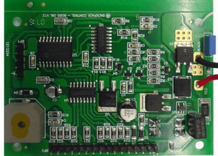
The solder mask bubbles.

One of the following reasons may cause PCB to carry water vapor:
Will
This PCB processing usually needs to be cleaned and dried before the next process For example, dry the solder mask after etching If the drying temperature is not enough at this time, water vapor will be brought into the next process, which will cause high temperature during welding Bubbles appear
The storage environment before PCB processing is poor, the humidity is too high, and the welding process is not dried in time;
Water containing flux is often used in wave soldering. If the PCB preheating temperature is not enough, the water vapor in the flux will enter the PCB substrate along the hole wall of the through-hole, and the water vapor will first enter around the pad., Bubbles will be generated after high temperature welding.
The solution is:
All links should be strictly controlLED. Purchased printed circuit boards shall be warehoused after inspection. Generally, PCB shall not bubble after 260 ℃/10s;
PCB shall be stored in a ventilated and dry environment, with a storage period of no more than 6 months;
The printed circuit board shall be pre baked in an oven at 120 ± 5 ℃/4h before welding;
The preheating temperature of wave soldering shall be strictly controlled and shall reach 100 ℃~150 ℃ before wave soldering. When using water containing flux, the preheating temperature should reach 110 ℃~155 ℃ to ensure that the water vapor can be completely volatilized.
Causes and solutions of blistering after PCB substrate welding
After SMA welding, nail sized bubbles appear The main reason is that the water vapor is entrained on the PCB substrate, which is especially suitable for the processing of multilayer boards. It is preformed by multi-layer epoxy prepreg and then hot pressed If the storage time of the epoxy resin prepreg is too short, the resin content is insufficient, and the prepreg is pre dried to remove the unclean water vapor, it is easy to carry water vapor after hot pressing, or the sEMI-solid film itself contains insufficient glue, and the adhesion between layers is insufficient, leaving an internal cause of blistering
In addition, after PCB purchase, due to the long storage period and humid storage environment, the chip was not pre baked in time before production, and this wet PCB chip is easy to blister.
Foaming of PCB board
Solution: After the PCB is purchased, it shall be accepted before warehousing; The printed circuit board shall be pre baked at (125 ± 5) ℃/4 hours before installation.
The above is the explanation given by the editor of pcb circuit board company.
If you want to know more about PCBA, you can go to our company's home page to learn about it.
In addition, our company also sells various circuit boards,
High Frequency Circuit Board and SMT chip are waiting for your presence again.
然后
联系
电话热线
13410863085Q Q

微信

- 邮箱


