QuICkly understand common terms of PCBA processing
As an employee of PCBA processing industry, in order to facilitate daily work, it is necessary to be familiar with common PCBA processing terms. This article lists some common professional terms and explanations of PCBA processing.
1、PCBA
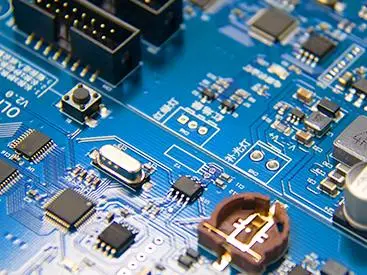
PCBA is the abbreviation of "Printed Circuit Board Assembly", which refers to a series of processing and manufacturing processes of PCB boards, such as SMT mounting, DIP plug-in, functional testing, and finished product assembly.
2. PCB board
PCB is the abbreviation of "printed circuit board". It usually refers to the circuit board, which is generally divided into single panel, double panel, and multilayer boards. Common materials include FR-4, resin, glass fiber cloth, and aluminum substrate.

3. Gerber files
Gerber files mainly describe the collection of file formats for drilling and milling data of PCB images (circuit layer, solder mask layer, character layer, etc.). When PCBA quotation is made, Gerber files need to be provided to PCBA processing plants.
4. BOM file
The BOM file is the bill of materials. All materials used in PCBA processing, including material quantity and routing, are important basis for material purchase. When PCBA quotations are made, they should also be provided to PCBA manufacturers.
5、SMT
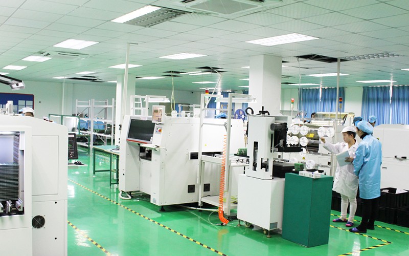
SMT is the abbreviation of "Surface Mounted Technology", which refers to the process of solder paste printing, chip element device mounting and reflow soldering on PCB.
6. Solder paste printing
Solder paste printing is the process of placing solder paste on the wire mesh, leaking solder paste through the holes on the wire mesh through the scraper, and accurately printing it on the PCB pad.
7、SPI
SPI is the solder paste thickness detector. After the solder paste is printed, SIP detection is required to detect the solder paste printing, so as to control the solder paste printing effect.
8. Reflow soldering
Reflow soldering is to send the pasted PCB board to the reflow welder. After the high temperature inside, the paste is heated into liquid, and finally cooLED and solidified to complete the welding.
9、AOI
AOI refers to automatic optical detection. The welding effect of PCB can be detected by scanning comparison, and the defects of PCB can be detected.
10. Rework
Repair the defective boards detected by AOI or manually.
11、DIP
DIP is the abbreviation of "dual in line package", which refers to the process of inserting components with pins on PCB, and then processing through wave soldering, leg shearing, post soldering, and board washing.
12. Wave soldering
Wave soldering is to send the inserted PCB into the wave soldering furnace and complete the welding of PCB through spraying flux, preheating, wave soldering, cooling and other links.
13. Scissor foot
Cut the legs of the components on the PCB board after welding to reach the proper size.
14. Post welding processing
Post welding processing is to repair and repair the PCB boards that are not completely welded after inspection.
15. Washboard
Plate washing is to clean the harmful substances such as flux left on the finished PCBA products, so as to reach the environmental standard cleanliness required by customers.
16. Three proofing paint spraying
Three proofing paint spraying is to spray a layer of special paint on the PCBA cost board. After curing, it can perform insulation, moisture-proof, anti electric leakage, shockproof, dustproof, anti-corrosion, anti-aging, mildew proof, anti loose parts, insulation and corona resistance. It can extend the storage time of PCBA and isolate external corrosion and pollution.
17. Pad
The turntable is a part of the widened PCB surface with no insulation paint covering, which can be used to weld components.
18. Encapsulation
Packaging refers to a packaging mode of components. Packaging is mainly divided into DIP dual in-line and SMD chip packaging.
19. Pin spacing
Pin spacing refers to the distance between the center lines of adjacent pins of the mounted components.
20、QFP
QFP is the abbreviation of "Quad flat pack", which refers to the surface mounted integrated circuit of plastic thin package with short wing leads on four sides.
21、BGA
BGA is the abbreviation of "Ball grid array", which refers to the integrated circuit device whose leads are arranged on the bottom of the package in a spherical grid shape.
22、QA
QA is the abbreviation of "Quality assurance", which refers to quality assurance. In PCBA processing, it often represents quality inspection to ensure quality.
23. Empty welding
There is no tin between the component pin and the bonding pad or there is no soldering due to other reasons.
24. False welding
The amount of tin between the component pin and the bonding pad is too SMAll, which is lower than the welding standard.
25. Cold welding
After the solder paste is solidified, there are fuzzy granular attachments on the bonding pad, which cannot meet the welding standard.
26. Wrong parts
The position of components is wrong due to BOM, ECN errors or other reasons.
27. Missing parts
If there is no component to be welded where the component should be welded, it is called missing.
28. Tin slag and tin ball
After PCB board is welded, there are surplus tin slag and tin balls on the surface.
29. ICT test
The open circuit, short circuit and welding of all components of PCBA are detected by contacting the test point with the test probe. It is characterized by SIMple operation, fast and accurate fault location.
30. FCT test
FCT test is often referred to as function test. By simulating the operating environment, PCBA is in various design states during operation, so that parameters of each state can be obtained to verify the function of PCBA.
31. Aging test
Aging test is to simulate the influence of various factors that may occur in the real use conditions of products on PCBA.
32. Vibration test
Vibration test is to simulate the anti vibration ability of components, parts and complete products in the use environment, transportation process and installation process. It is used to determine whether the product can withstand various environmental vibrations.
33. Finished product assembly
Assemble the PCBA, shell and other parts after the test to form the finished product.
34、IQC
IQC is the abbreviation of "Incoming Quality Control", which refers to the quality inspection of incoming materials and the quality control of purchased materials by the warehouse.
35. X-Ray detection
X-ray penetration can be used to detect the internal structure of electronIC components, BGA and other products, as well as the welding quality of solder joints.
36. Steel mesh
The steel mesh is a special mold for SMT. Its main function is to help the deposition of solder paste, so as to transfer the exact amount of solder paste to the exact position on the PCB.
37. Fixture
Fixtures are products that need to be used in the mass production process. With the help of fixture production, production problems can be greatly reduced. Fixtures are generally divided into three categories: process assembly fixture, project testing fixture and circuit board testing fixture
38、IPQC
Quality control in PCBA production process.
39、OQA
Quality inspection of finished products before delivery.
40. DFM manufacturability inspection
Optimize the design and manufacturing principles, process and accuracy of components of products. Avoid product manufacturing risks.
These are 40 commonly used professional terms about PCBA processing, which is convenient for PCBA practitioners to understand the industry of PCBA processing more quickly. After understanding these commonly used terms, it is also more convenient to communicate with customers, factories and PCB designers in many aspects.
然后
联系
电话热线
13410863085Q Q

微信

- 邮箱


