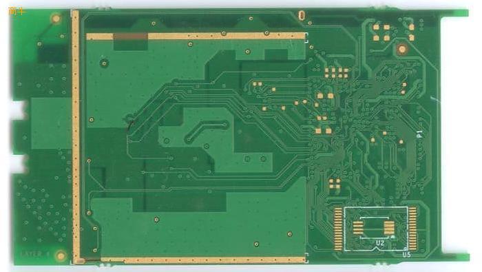
When PCB is to be processed, PCB is transmitted on SMT production line through guide rail. Therefore, a pair of edges of cloth forbidden components must be reserved as the transmission edge. Usually, the two long edges of PCB or the rear panel are used as its transmission edges.
The width of the fixed plate of the SMT transmission track is 3.0mm, and the theoretICal limit value of the transmitting edge is 3.0mm. However, it is recommended that you do not follow this limit to increase the difficulty of mounting. To reserve more blank space as margin, it is recommended to use 5.0mm as the "forbidden cloth area" at the transmission edge.
If the cloth prohibition margin is insufficient, the interference part will affect the solder paste or the placed components after the PCB is mounted to the transmission guide rail. The interference part on the board edge can only be post soldered or requires additional fixtures to increase the production cost.

If the distance between the patch part in the plate and the plate edge is far enough to not be within the caterpillar range, then no additional process edge is required. If the part is within the caterpillar range, process edge must be added as the edge clamping area. According to the characteristics of the machine, the width of the process edge is usually 3-10mm, with 5mm being the most common.
Generally, the process edge is added on the longer side, and the board enters the SMT machine vertically. In this way, the hardness of the board is relatively high, and the chip will not bounce due to the light pressure of the machine probe. However, the process edge area of the lengthened side is more, which increases the average price of a single board in a disguised way. If the hardness of the board is enough, it can be added in the short direction, the process edge area is SMAll, the average cost of a single board is reduced, and the board enters the SMT machine crosswise.
SMT usually uses MARK points for alignment. If there is no MARK point in the board, 2-4 MARK points must be added at the opposite corners of the process edge. The size of the MARK point is generally 1.0mm. The exposed copper is coated with tin. In some cases, the process edge can be added or not.
During production, positioning is required for forming and testing. The special positioning hole is added at the process side to make a relatively standard shape and facilitate positioning. Therefore, 3-4 locating holes with a diameter of 2.0-4.0mm will be added at the process edge, with a diameter of 3mm being the most common and the best
Precautions for PCB process edge design:
No patch or machine inserted PCB components can be arranged in the process edge, and the entities of the patch or machine inserted components cannot enter the process edge and above.
The entities of hand inserted components shall not fall in the space within 3mm above the upper and lower process edges, and shall not fall in the space within 2mm above the left and right process edges.
The conductive copper foil in the process side shall be as wide as possible. The lines less than 0.4mm need to be strengthened with insulation and wear resistance treatment, and the line at the extreme edge shall not be less than 0.8mm.
The process edge and PCB can be connected by stamp hole or V-shaped slot, generally V-shaped slot is selected.
There shall be no bonding pad or through hole on the PCB process edge.
Area greater than 80 mm ² The PCB must have a pair of parallel process edges, and there is no component entity in the upper and lower space of the process edges. The width of the process edge can be appropriately increased according to the actual situation.
然后
联系
电话热线
13410863085Q Q

微信

- 邮箱


