Anti interference design of Train High Speed Digital PCB
The problems that should be paid attention to in the design of high-speed digital circuit are detaiLED in the printed circuit board, whICh aspects will be affected by the high-speed digital circuit in the train on-board system, and the reasons for these impacts Several methods should be adopted The practice proves that the circuit designed by these methods can greatly improve the anti-interference efficiency of the product With the continuous development of science and technology, the train is also developing at a high speed. The on-board system of the train gradually adopts high-speed digital circuits There are many interference sources on the train, including electromagnetic interference generated by various transformers, fans, pantograph, air compressor, etc, Affect the normal operation of high-speed digital circuit of the train In addition, in order to ensure the comfort of the riding environment and working environment, the car is also equipped with various electrical equipment, such as air conditioners, electric heaters, ventilators, etc, It will also generate electromagnetic radiation outside, affecting the normal operation of high-speed digital circuits Therefore, in such a complex train environment, how to ensure the reliability of high-speed digital signals will become particularly important If these problems are not handled properly, it will lead to signal distortion, timing error, system instability and many other situations, which will bring incalculable losses In order to ensure the normal operation of train communication, the anti-interference design of control and other systems is as important as the functional design At the beginning of the design, we must consider the suppression of digital circuit interference, otherwise it is difficult to meet the anti-interference requirements of high-speed digital circuits Therefore, it is necessary to improve the anti-interference ability of the digital circuit board, reduce the circuit radiation, and avoid taking remedial measures for the anti-interference of the circuit board after the design is completed
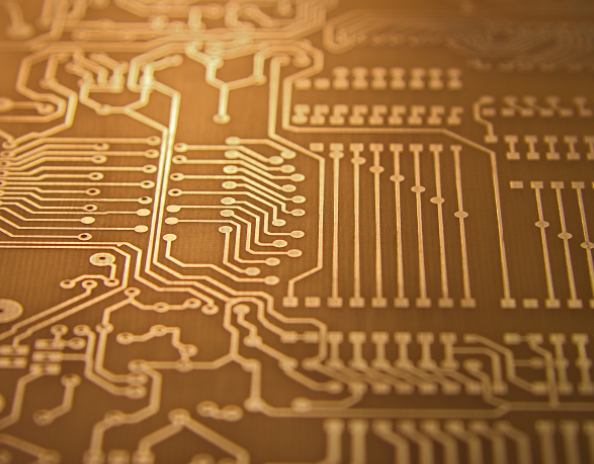
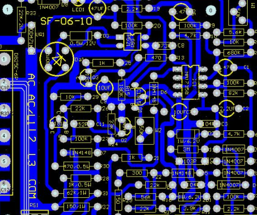
Printed circuit board

1. The way of interference
There are three basic ways of interference formation: interference source, coupling path, and sensitive source These aspects are described below
1.1 Interference coupling path PCB board
The interference on the circuit board mainly includes common mode interference and differential mode interference Differential mode interference is generated by signal loop, and common mode interference is generated by common mode current on cable For printed circuit boards, it mainly refers to differential mode interference, because the frequency range of differential mode interference is the entire frequency band occupied by circuit signals Various interferences affect the normal working system The main method to reduce differential mode interference is to minimize the track length and reduce the signal loop area during routing
1.2 Generation method of interference source PCB
The main causes of various types of interference in high-speed digital circuits are the inherent noise frequency of the power supply itself, various changes in di/dt and dt on du/external circuits Various capacitive and inductive loads on the line, so when the signal jumps, it will produce SPIkes to form noise, which will be conducted along the circuit through the current loop of each circuit. In this case, the inherent noise of the power supply itself and various noises caused by high-speed digital conversion Decoupling and filtering are the best methods to suppress the noise generated by the circuit itself or various types of abrupt signals This not only reduces its own noise, but also absorbs the influence of the outside world and improves its anti-interference ability
1.3 sensitive source PCB boards
The sensitive source of high-speed digital signal mainly refers to objects vulnerable to external interference, such as A/D, D/A converter, logic controller, microcontroller, crystal oscillator, digital integrated circuit, weak signal amplifier, etc The stability of these devices is directly related to the stability and accuracy of circuit board system operation Therefore, these sensitive sources must be properly protected to improve their anti-interference capability
2. Improve the anti-interference measures of the system PCB board
2.1 Reduce the coupling loop
The main method to reduce coupling is to reduce the signal loop area
1) Reduce the ground wire and power coupling loop
The ground wire impedance is the main cause of the ground wire noise on the circuit board For high-speed digital circuit boards, multi-layer boards should be used to reduce the loop area. The middle layer should be used as the power layer or grounding layer. The distance between the layers adjacent to the power supply and the ground should be as SMAll as possible; Make each signal layer have corresponding grounding. The area of the ring formed by the signal line and its grounding loop shall be as small as possible The smaller the annular area, the less external interference In view of this feature, when dividing the ground plane, we should consider the distribution of ground plane and important signal tracks to prevent problems caused by ground plane slotting, etc, The signal line shall not pass through the separation area between the ground plane and the power plane to prevent the formation of a large grounding loop At the same time, the power supply layer should be retracted from the ground layer by about 3 mm, so that more than 70% of the power interference can be suppressed
2) Reduce the coupling loop of the sensitive source signal
For sensitive signals such as periodic signals, such as clock signals, analog signals, and low order signals of address bus, the interference is very strong, which is also the key to design high-speed digital circuits The wiring of key signals on the printed board should be routed according to the principle of high to low (sorting method: high to low: analog signal - reset signal - I2C - clock signal - read and write signal - high speed, radio frequency signal - data bus - address bus ); the key signal wiring should go to the inner layer as far as possible; and a small capacitor should be connected in parallel for filtering; the signal layer can be routed in parallel only through the two layers separated by the ground plane; the signal line should be as short as possible; The components of the high frequency connection on the printed board should be as close to the traces as possible to reduce the distribution parameters and electronic interference of high frequency signals, so as to improve the anti-interference ability of sensitive signal sources
3) Reduce the coupling loop at the edge of the circuit board
Whether the edge processing of the printed circuit board is reasonable determines whether the external interference of the signal can be suppressed more effectively. In order to prevent high-speed digital circuit from interfering with the outside through the edge of the circuit board, its wiring position should be strictly controlled and it should be as close to the inside of the printed board as possible The signal line with strong interference (such as high frequency) shall not reach the edge of the circuit board to prevent the leakage of external interference caused by the lack of corresponding grounding coupling circuit
2.2 Suppress interference sources
Suppressing the interference source is to reduce the influence of the interference source du/dt and di/as many dt as possible Reducing the dt of du/interference source is mainly realized by connecting capacitors in parallel at both ends of the interference source and adding decoupling and filtering Reducing the dt of di/interference source is mainly realized by connecting inductance and interference source in series or adding freewheeling diode For example, adding a continuous current diode to the relay can eliminate the back EMF interference when the coil is disconnected
1) Increase the decoupling capacitor
The decoupling capacitor takes the interference of the output signal as the filtering object. Adding a parallel decoupling capacitor in the chip can eliminate the self-excited power supply and suppress the influence of level change, which can make the power supply noise and the influence of level change return to the ground wire in a short path to improve the anti-interference capability In order to better suppress noise, each chip should be equipped with a decoupling capacitor as close as possible to the power and ground pins of the chip The value of decoupling capacitor is usually 0.01-0.1 degrees Fahrenheit, which can be C=1/F. That is, 0.1 degrees Fahrenheit for 10MHZ and 0.01 uf for 100MHZ. The higher the frequency, the smaller the decoupling capacitor value
2) circuit filter absorption
Corresponding filtering forms should be adopted for the mutation signals that are prone to burrs to suppress the high-frequency burrs generated by the mutation of high-speed signals. The filtering method usually uses passive component capacitors or inductors with resistors, and uses their energy storage characteristics for voltage and current to achieve the purpose of filtering RC filter circuit is usually used When the voltage rises suddenly, parallel capacitor C can store energy. When the voltage drops, the energy is released. In this case, the load filtered voltage is relatively smooth and high-frequency noise is reduced However, in order not to affect the normal high-frequency signal waveform, the value should not be too large, and small capacitors should be used as far as possible According to the total impedance of the circuit and the bandwidth and rise time of high-frequency signal, the selection size of filter capacitor C is based on calculation and experience Refer to Table 1 below: The higher the operating frequency of the system, the smaller the value of the filter capacitor
3. Conclusion
The reliability of the anti-interference design of high-speed digital circuits has a profound impact on the overall performance of the entire electronic and electrical equipment. The reliability of any product should start from the source of design Only mastering the reliability design of printed circuit can ensure the reliability of products Reliability, truly improve the reliability of printed boards It can be seen from various figures that the high-speed digital printed circuit board improved by this method can reduce the noise generated by itself and improve its anti-interference ability Considering the economic consideration of R&D cost, and considering that the printed circuit board will save a lot of repeated design costs in the early stage of design
然后
联系
电话热线
13410863085Q Q

微信

- 邮箱


