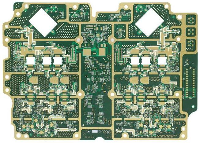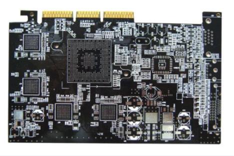
Some Requirements for PCB Layout in High Quality PCB Design
In order to ensure the quality of PCB design, when designing PCB, it should be noted that the PCB drawing meets the requirements
1 Component layout
Reasonable arrangement of components is this basIC promise of designing a high quality PCB layout Component layout requirements mainly include installation, force, heat, signal, and aesthetics
1.1. Installation
Refers to a series of basic requirements for the smooth installation of the PCB board into the main housing, bushing, and slot in specific applications to avoid space interference, short circuit and other accidents, and keep the designated connector at the designated position on the main housing or housing requirement. I won't go into details here
Printed circuit board

1.2. Force
The circuit board should be able to withstand various external forces and vibrations during installation and work. Therefore, the PCB should have a reasonable shape, and the positions of various holes (screw holes, special shaped holes) on the board should be reasonably arranged In general, the distance between the hole and the edge of the plate should be at least greater than the diameter of the hole At the same time, it should be noted that the weak part of the plate caused by the special-shaped hole should also have sufficient bending strength In particular, connectors that "extend" directly from the equipment housing on the board shall be properly fixed to ensure long-term reliability
1.3. Heat
For high power devices with serial heat generation, in addition to ensuring heat dissipation conditions, it should also be placed in an appropriate position Especially in complex analog systems, special attention should be paid to the adverse effects of temperature fields generated by these devices on fragile preamplifier circuits Generally, components with very high power shall be made into separate modules, and certain thermal isolation measures shall be taken between them and signal processing circuits
1.4. Signals
Signal interference is an important factor to be considered in PCB layout design. Several basic aspects are: weak signal circuit and strong signal circuit are separated or even isolated; The AC part is separated from the DC part; The high frequency part is separated from the low frequency part; Pay attention to the direction of the signal line; Layout of ground wire; Measurement These have been repeatedly emphasized in a large number of papers, and will not be repeated here
1.5. Beautiful
It is not only necessary to consider the near and orderly placement of components Because ordinary laymen sometimes emphasize the former, in order to one-sided evaluate the advantages and disadvantages of circuit design, when the performance requirements are not strict, the former should be given priority to the product image However, in high-performance occasions, if a double-sided board must be used, the circuit board is also packaged in it. It is usually invisible, and the aesthetics of traces should be given priority The next section will discuss the "aesthetics" of cabling in detail
2. Wiring principles
Some anti-jamming measures not commonly found in the literature are detaiLED below. Considering that a large number of double-sided panels are still used in practical applications, especially in the trial production of products, the following contents mainly focus on double-sided panels
2.1. Wiring "Aesthetics"
When turning, avoid right angles and try to use diagonal lines or arcs for transition The wiring should be orderly and centrally arranged, which not only avoids mutual interference of signals of different properties, but also facilitates inspection and modification For digital systems, there is no need to worry about interference between signal lines (such as data lines and address lines) of the same CAMp, but the control signals, such as read and write, should be isolated and protected by a ground wire In a large area (discussed further below), try to maintain a reasonable and equal distance between the ground wire (in fact, it should be the ground "surface") and the signal wire For weak current system, ground wire and power wire shall be as close as possible For systems using surface mount components, the signal line should go all the way to the front
2.2. Ground wire arrangement
There are many discussions on the importance and layout principles of the ground wire in the literature My experience is that in order to improve the reliability of the system (her than just making an experimental prototype) To this end, we must spare no effort to implement the principle of "paving roads in large areas" When laying the ground, it must generally be grid shaped, unless these scattered places are separated by other lines The thermal efficiency and high frequency conductivity of grid grounding are far superior to the whole grounding wire In double-sided wiring, sometimes the ground wire must be separated in order to arrange the signal line, which is extremely unfavorable to maintain a sufficiently low ground resistance To this end, a series of "SMArt" methods must be used to ensure that the ground current is "smooth" These techniques include: extensive use of surface mount components to eliminate the space "should" belong to the ground Make full use of the front space: In the case of using a large number of surface mounted components, try to make the signal line reach the top layer, and hand the bottom layer to the bottom layer "selflessly". This involves countless tips. I write a PCB skill myself: there is a skill in switching pins, and there are many SIMilar spells, which will be written one by one in the future Reasonably arrange signal lines and "give" important areas on the board of directors, especially the "hint" (this is related to the communication of the entire board ground line) to the ground line. As long as carefully designed, this can still be done Forward backward coordination: sometimes the grounding wire is "impossible" on one side of the board. Then you can try to make the wiring on both sides coordinate with each other And then pass through enough and reasonably located vias (considering that the vias have a large resistance) Forcibly separated, but reluctantly looking forward to reunification, the two sides of the Taiwan Strait are connected as a whole and have sufficient conductivity The meaning of the dog jumping over the wall: When the huge ground wire cannot be found and is unwilling to be cut off by a signal wire, let the signal express dissatisfaction and use jumper wires Sometimes, I don't want to pull only one bare wire. The signal just passes through the resistor or other "long leg" devices. I can reasonably expand the pin of this device so that it has dual functions as a jumper, not only transmitting signals, but also avoiding using inappropriate jumper names Of course, in most cases, I can always let such signals pass through the right place and avoid crossing with the ground wire, which requires observation and imagination Minimum principle: the grounding current path shall be reasonable, and large current and weak signal current shall not move side by side Sometimes, it is unreasonable to choose a reasonable path and a row of grounding wires for an army By the way, there is a famous saying: "You can trust your mother, but never trust your position" In the case of extremely weak signal processing (below microvolts), even if the average value is guaranteed to maintain the consistency of ground potential, the ground potential difference of key points on the circuit still exceeds the amplitude of the signal being processed, at least by the same order of magnitude Even if the electrostatic potential is appropriate, the transient potential difference may still be large It is applicable to such occasions. First of all, in principle, the operation of the circuit should be as independent of the ground potential as possible
然后
联系
电话热线
13410863085Q Q

微信

- 邮箱


