鑫景福致力于满足“快速服务,零缺陷,辅助研发”PCBA订购单需求。


PCB layout and quality analysis of high-speed signal boards are undoubtedly the focus of discussion among PCB engineers. In partICular, the working frequency of today's circuit boards is getting higher and higher. For example, the application frequency of general digital signal processing (DSP) circuit boards is very common in 150-200MHz. It is not surprising that CPU boards have reached more than 500MHz in practical applications. The design of Ghz circuits has been very popular in the communication industry. The design of all these PCB boards is often realized by using Multilayer board technology. It is inevitable to adopt PCB design technology of power supply layer in multilayer Board Design. In the power layer design, the design is often very complicated due to the mixed application of multiple types of power supplies.
What are the problems that haunt PCB engineers? How to define the number of PCB layers? How many layers are included? How to arrange the content of each layer in the most reasonable way? For example, how many layers should there be, and how the signal layer and stratum are alternately arranged.
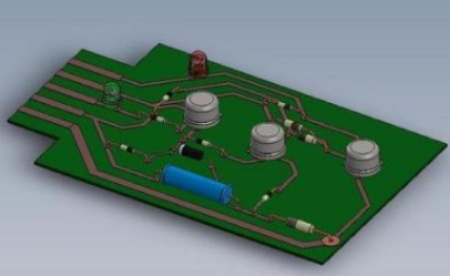
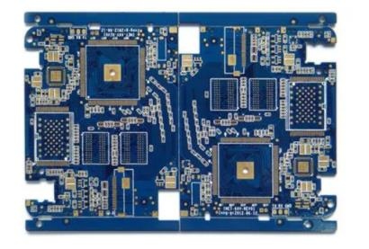
High speed signal board
How to design multiple power block systems? Such as 3.3V, 2.5V, 5V, 12V, etc. The reasonable division and common ground of power layer is a very important factor for PCB stability.
How to design decoupling capacitor? Using decoupling capacitors to eliminate switching noise is a common method, but how to determine its capacitance? Where is the capacitor placed? When to use what type of capacitor, etc.
How to eliminate ground bounce noise? How does ground missile noise affect and interfere with useful signals? How to eliminate the return path noise? In many cases, unreasonable loop design is the key to the failure of the circuit, and loop design is often the most helpless work for engineers.
How to reasonably design the current distribution? Especially, it is very difficult to design the current distribution in the geoelectric layer, and if the total current is distributed unevenly in the PCB, it will directly and significantly affect the unstable operation of the PCB.
In addition, there are some common singularities such as overshoot, undershoot, ringing (oscillation), time delay, impedance matching, burr, etc., but these problems are inseparable from the above problems. There is a causal relationship between them.
In general, to design a high-quality high-speed signal board, two aspects should be considered: signal integrity (SI) and power integrity (PI). Although the direct result is from the signal integrity, we must not neglect the design of power supply integrity. Because the power supply integrity directly affects the final signal integrity.
There is a big mistake among PCB engineers, especially those who used traditional EDA tools to design high-Speed PCB. Many engineers have asked us: "Why are the results analyzed by the SI signal integrity tool of EDA inconsistent with the actual test results of our instruments, and the analysis results are often ideal?" In fact, this question is very SIMple. The reasons for this problem are: on the one hand, the EDA manufacturer's technicians did not explain it clearly; On the other hand, it is the understanding of PCB designers to the simulation results. As we know, EDA tools used more frequently in the Chinese MARKet are mainly (signal integrity) analysis tools. SI is based on wiring and device models without considering the influence of power supply, and most of them do not even consider analog devices (assumed to be ideal). It is conceivable that such analysis results and actual results must be error. Because in most cases, the impact of power integrity in PCB is more serious than SI.

抖音二维码

Q Q二维码

微信二维码
点击
然后
联系
然后
联系
电话热线
13410863085Q Q

微信

- 邮箱