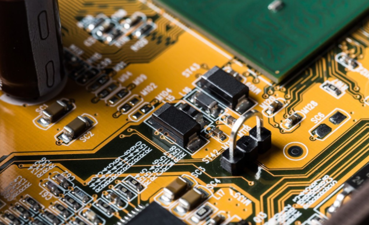
PCB design errors and PCB quality acceptance criteria
PCB design error
1. PCB process has no edges and process holes, whICh cannot meet the clamping requirements of SMT equipment, that is, it cannot meet the requirements of mass production.
2. The shape of PCB is abnormal or the size is too large or too SMAll, which cannot meet the clamping requirements of the equipment.
3. There is no optical positioning MARK around PCB and FQFP pad, or the marking point is non-standard. For example, there is a welding mask around the marked point, or it is too large or too small, which causes the contrast of the marked point image to be too small, and the machine alarms frequently. work
4. The size of cushion structure is incorrect. For example, the pad spacing of the wafer component is too large or too small, and the pads are asymmetric, resulting in defects such as skew and tombstone after the wafer component is welded.
5. There are through holes on the pad, which will cause the solder to melt and leak to the bottom layer through the through holes during welding, resulting in too little solder in the solder joint.
6. The pad size of the wafer assembly is asymmetric, especially the ground wire and some wires are used as the pad, which makes the pads at both ends of the wafer assembly heated unevenly in the reflow soldering process, and the solder paste melts continuously to form a tombstone. Disadvantages
Circuit board

7. IC pad design is incorrect. The pad in FQFP is too wide, resulting in bridging after welding, or the trailing edge of the pad is too short, resulting in insufficient strength after welding.
8. The interconnection wires between the bonding pads of integrated circuits are centered, which is unfavorable to the inspection of SMA after welding.
9. IC has no auxiliary pad during wave soldering, which leads to bridging after welding.
10. PCB thickness or IC distribution in PCB is unreasonable, and PCB is deformed after welding.
11. The design of test points is not standardized, and ICT cannot work.
12. The clearance between SMDs is incorrect, which is difficult to repair in the future.
13. The welding mask and character mapping are not standardized. The welding mask and character mapping fall on the pad, causing false soldering or power disconnection.
14. The design of the circuit board is unreasonable, such as the poor processing of the V-groove, which leads to PCB deformation after reflow soldering.
One or more of the above errors will appear in the products with poor design, which will affect the welding quality to varying degrees. One of the reasons for poor design is that designers do not know enough about SMT process, especially the "dynamic" process of components during reflow soldering. In addition, neglecting the participation of craftSMEn in the early design stage and the lack of manufacturability design specifications in enterprises are also the reasons for poor design.
In which aspects do PCB quality acceptance standards include?
PCB quality acceptance standard
PCB quality acceptance shall include design, process and full approval. Generally, test welding, sample sealing and batch supply shall be carried out first, including the following aspects:
1. Power connection efficiency. It is usually self checked by the PCB manufacturer, and the test instruments used are:
Lamp board tester (continuity tester). It can measure the opening and closing of the connection, and whether the logical relationship of the Multilayer board including the metallized hole is correct.
Automatic optical tester for pattern defects. You can view the overall performance of PCB, including lines, characters, etc.
2. Manufacturability. Including appearance, smoothness, flatness, character cleanliness, through-hole resistivity, power efficiency, heat resistance, weldability and other comprehensive efficiency.
PCB surface shall be free of residual flux, glue and other oil stains. There is no short circuit or open circuit.
The non line conductor (residual copper) must be more than 2.5mm away from the line, and the area must be – 0.25mm2
The drilling shall be free of over drilling, missed drilling, deformation and through hole impermeability.
It is not allowed to bend the circuit and bonding pad; The circuit is not allowed to contact copper and tin.
PCB is not allowed to break; If the circuit board needs VCUT, its depth must be deeper than 1/3 of the circuit board thickness.
The actual circuit width shall not deviate from the original design width by ± 20%; The shape tolerance is ± 0.15 mm; The convexity or unevenness of the substrate edge is less than or equal to 0.2mm.
The offset of solder mask wire mesh shall not exceed ± 0.15 mm; No fingerprints, waterlines or wrinkles are allowed on the surface of solder mask.
The characters on the surface of components shall not be damaged or unrecognizable; The painted area on the pad must be - 10% of the original area.
The degree of PCB deformation, bending and warping is less than or equal to 1% of the diagonal length of the substrate
After PCB quality acceptance, vacuum packaging machine is generally used for vacuum packaging of products. Its purpose is to prevent dust and moisture, thus extending the storage period. Generally speaking, its weldability can still be kept good after 1 to 2 years of storage.
What are the common PCB design errors, their causes and PCB quality acceptance criteria?
然后
联系
电话热线
13410863085Q Q

微信

- 邮箱


