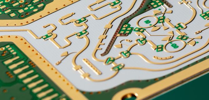
Understand the technology and basIC information of FPC
The basic composition information of FPC is the base film or heat-resistant resin constituting the base film, followed by the copper clad plate and protective layer constituting the conductor
Base film information FPC ranges from the initial polyimide film to the heat-resistant film that can withstand welding The first generation of polyimide film has the problems of high hygroscopicity and large thermal expansion coefficient. In retrOSPect, the second generation of polyimide information is used in high-density PCB circuits
Copper clad plate
Many FPC manufacturers usually purchase in the form of CCL, and then use CCL as the starting material to process them into flexible PCB products. FPC copper clad laminate or protective film (coating film) using the first generation polyimide film is made of an adhesive, such as epoxy or acrylic resin. The heat resistance of the adhesive used here is lower than that of the polyimide, and the heat resistance or other physical properties of the FPC are limited.
In order to avoid the disadvantages of traditional adhesive based CCL, high-performance FPCs including high-density circuits use adhesive free CCL. So far, there are many manufacturing methods, but the following three methods can be used in practice:
Circuit board

1) PCB casting process
The casting process starts with copper foil. The liquid polyimide resin is directly coated on the surface active copper foil and heat treated to form a film. The polyimide resin used here must have good adhesion to copper foil and good dimensional stability, but no polyimide resin can meet these two requirements. First, a thin layer of polyimide resin (adhesive layer) with good adhesion is coated on the surface of active copper foil, and then a certain thickness of polyimide resin with good dimensional stability is coated on the adhesive layer (core layer). Due to the different thermophysical properties of these polyimide resins, if the copper foil is etched, large pits will appear in the base film. In order to prevent this phenomenon, an adhesive layer is coated on the core layer to obtain good symmetry of the base layer.
In order to manufacture double-sided copper clad laminate, the adhesive layer uses thermoplastic (hot melt) polyimide resin, and then the copper foil is laminated on the adhesive layer by hot pressing.
2) Sputtering/electroplating process
The starting material of sputtering/electroplating process is a heat-resistant film with good dimensional stability. The first step is to use the sputtering process to form a seed layer on the surface of the activated polyimide film. The seed layer can ensure the bonding strength with the conductor base layer, and at the same time, it plays the role of electroplating the conductor layer. Nickel or nickel alloys are usually used. To ensure conductivity, a thin layer of copper is sputtered on a nickel or nickel alloy layer, and then copper is plated to the specified thickness.
3) Hot pressing method
The hot pressing method is to coat thermoplastic resin (thermoplastic adhesive resin) on the surface of heat-resistant polyimide film with good dimensional stability, and then laminate the copper foil on the hot melt resin at high temperature. Composite polyimide film is used here.
This composite polyimide film can be purchased from professional manufacturers, and the manufacturing process is relatively SIMple. When manufacturing copper clad laminate, the composite film and copper foil are laminated together and hot pressed at high temperature. The equipment investment is relatively SMAll, suitable for small batch and multi variety production. The double-sided copper clad laminate is also easier to manufacture.
Another important data element that constitutes the FPC is the protection layer (overlay), and various protection data have been proposed. The first practical protective layer is to apply the same heat-resistant film as the base material and use the same adhesive as the CCL. This structure is characterized by good symmetry and still occupies the main part of the MARKet, usually referred to as "film coating". However, this kind of film protective layer is difficult to automate the processing, which increases the overall manufacturing cost. Because it is difficult to perform fine window processing, it cannot meet the demand of high-density SMT that has become the mainstream in recent years.
In order to meet the requirements of high-density installation, photosensitive protective layer has been adopted in recent years The process of coating a copper foil circuit with photosensitive resin, and then using PCB lithography to open a window in the necessary part Photosensitive resin materials are available in liquid form and dry film form At present, the protective coatings based on epoxy resin or acrylic resin have been put into practical use, but their physical properties, especially their mechanical efficiency, are far inferior to those based on polyimide In order to improve this situation, it is necessary to use polyimide resin or improve the physical properties of the PCB protective layer data based on epoxy resin or acrylic resin, or improve the PCB process The photosensitive polyimide resin used here is expected to be used as interlayer insulating material in the process of multilayer circuit formation
然后
联系
电话热线
13410863085Q Q

微信

- 邮箱


