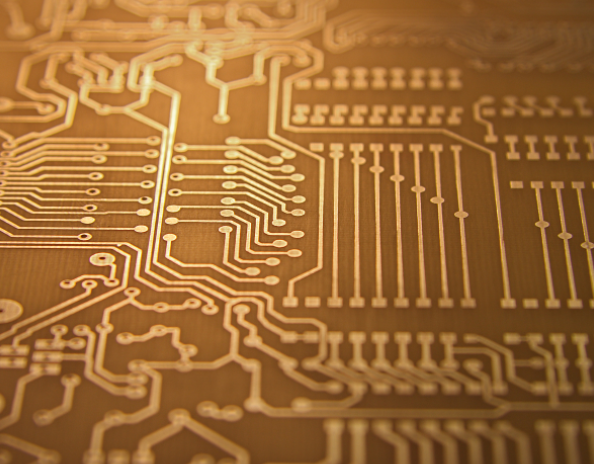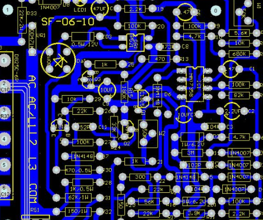
Ground treatment PCB surface technology
With the continuous improvement of human requirements for living environment, the current environmental issues involved in PCB production process are partICularly prominent At present, lead and bromine are the most popular topics; Lead free and halogen-free will affect the development of PCB in many aspects Although at present, the change in PCB surface treatment process is not very big, which seems to be a relatively remote matter, it should be noted that long-term slow changes will lead to huge changes With the increasing demand for environmental protection, the surface treatment process of PCB will change dramatically in the future
How to "keep pace with the times" to deal with PCB surface technology?
Purpose of surface treatment
The basic purpose of surface treatment is to ensure good weldability or electrical efficiency. Since natural copper often exists in the air in the form of oxide, it is unlikely to maintain the original copper state for a long time, so it is necessary to conduct other treatment for copper. Although the strong flux can be used to remove most of the copper oxides in subsequent assembly, it is not easy to remove the strong flux itself. In general, the industry does not use strong flux.
Five common surface treatment processes
There are many PCB surface treatment processes, such as hot air leveling, organic coating, chEMIcal nickel plating/immersion gold, immersion silver and immersion tin, which will be introduced one by one below
1. Hot air leveling
Also known as hot air solder leveling, it is a process of coating molten tin lead solder on the PCB surface and flattening (blowing) it with heated compressed air to form a copper oxide resistant coating with good solderability. Cladding. In the process of hot air leveling, copper tin intermetallic compound is formed at the joint between solder and copper. The thickness of solder used to protect the copper surface is approximately 1-2 mils. During hot air leveling, PCB shall be immersed in molten solder; Before the solder is solidified, the air knife blows the liquid solder; The air knife can minimize the meniscus of solder on the copper surface and prevent solder bridging. There are two types of hot air leveling: vertical and horizontal. It is generally believed that the horizontal type is better. The main reason is that the leveling of horizontal hot air is more uniform and can realize automatic production.
The general process of hot air leveling process is: micro etching, preheating, coating, flux spraying, tin cleaning.
Circuit board

2. Organic coating process
Different from other surface treatment processes, it is a barrier between copper and air; Organic coatings are widely used in industry due to their SIMple process and low cost. The early organic coating molecules are imidazole and benzotriazole, which play a role in rust prevention, while the latest molecule is mainly benzimidazole, which is copper, which chemically bonds nitrogen functional groups to PCB. In the subsequent welding process, if there is only one organic coating on the copper surface, it will not work, and there must be many layers. This is why liquid copper is usually added to the chemical tank. After coating the first layer, the coating layer adsorbs copper; Then the organic coating molecules of the second layer are combined with copper until twenty or even hundreds of organic coating molecules are gathered on the copper surface, which can ensure that multiple loops are performed. Flow welding.
The test shows that the latest organic coating process can maintain good performance in a variety of lead-free welding processes.
The general process of the organic coating process is: degreasing micro etching pickling pure water cleaning organic coating cleaning. This process is easier to control than other surface treatment processes.
3. Electroless nickel plating/gold leaching Electroless nickel plating/gold leaching process
It is not as simple as organic coating Electroless nickel plating/gold immersion seems to add a thick layer of armor on PCB; In addition, unlike organic coatings, the electroless nickel/gold plating process does not serve as a rust barrier, and it can be used on PCB for a long time. The process is very useful and achieves good power efficiency Therefore, the purpose of electroless nickel plating/gold DIPping is to wrap a thick layer. The copper surface has good electric nickel gold alloy, which can protect PCB for a long time; In addition, it also has the environmental protection that other surface treatment processes do not have Patience
The reason for nickel plating: Since gold and copper will diffuse each other, the nickel layer can prevent the diffusion between gold and copper. In addition, electroless nickel plating/gold immersion can also prevent copper dissolution, which will benefit lead-free assembly.
The general process of electroless nickel plating/gold leaching process is: pickling, micro etching, pre leaching, activation, electroless nickel plating, and electroless gold leaching. There are mainly 6 chemical tanks, involving nearly 100 kinds of chemicals. It is difficult to control this process.
然后
联系
电话热线
13410863085Q Q

微信

- 邮箱


