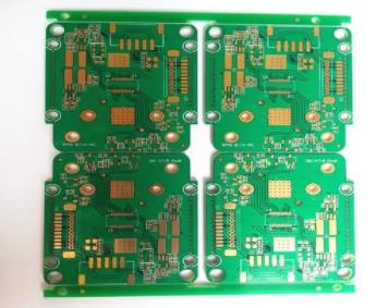
After PCB design and wiring, due to the requirements of pcb design and assembly, it is necessary to carry out panel design for some PCBs with special shapes, so that the subsequent PCB assembly process can be carried out smoothly. In the process of panel assembly design, it is usually necessary to add sidebars and connect one or several PCB units with the sidebars in a certain way to form a PCB shape that meets the assembly requirements. The size of the panel will have a direct impact on the material utilization rate and the size of the production panel, and even signifICantly affect the price of PCB. The number, width, position of the edges, the number of PCB units, the arrangement of PCB units, the connection method, and the slot width will all affect the panel size.

This paper mainly discusses how to optimize the size of the panel by controlling these influencing factors in the process of panel design, on the prEMIse of meeting the requirements of pcb and pcb assembly process, so that it can generate high panel utilization and appropriate production panel size when forming PCB production panel, thus obtaining a lower size.
The pcb must be assembLED
In the following cases, PCBs need to be assembled to form a panel to meet the PCB process assembly requirements:
(1) Mechanical structure requirement of PCB design itself
(2) The component bonding pad is too close to the PCB edge, the top layer is less than 4.06 mm, and the bottom layer is less than 5.08 mm (the top layer is less than 0.16 inch, and the bottom layer is less than 0.2 inch)
(3) The edge of the test point to be soldered is too close, the top layer is less than 4.06 mm, the bottom layer is less than 5.08 mm (the top layer is less than 0.16 inch, the bottom layer is less than 0.2 inch)
(4) Irregular shape or size is too SMAll to pass the assembly line smoothly
(5) To improve the efficiency of PCB assembly production process
Strictly follow the PCB design process to assemble, which can greatly save costs and achieve more ideal PCB board making results.
pcb board design and manufacturing process
print circuit board: print the printed circuit board with transfer paper, pay attention to the sliding side facing yourself, and generally print two circuit boards, that is, two circuit boards are printed on one sheet of paper. Select the PCB with the best printing effect.
Cut the copper clad plate, and use the light-sensitive plate to make the whole process diagram of the circuit board. The copper clad plate, that is, the circuit board with copper film on both sides, is cut into the size of the circuit board, not too large, to save materials.
Pretreatment of CCL: Polish the oxide layer on the surface of the CCL with fine sandpaper to ensure that the carbon powder on the thermal transfer paper can be firmly printed on the CCL when the circuit board is transferred. The polished standard is that the board is bright without obvious stains.
Transfer circuit board: cut the printed circuit board to an appropriate size, paste the printed side of the circuit board on the copper clad plate, and put the copper clad plate into the thermal transfer machine after alignment. Make sure that the transfer paper is not misplaced when putting it in. Generally speaking, after 2-3 times of transfer, the circuit board can be firmly transferred to the copper clad laminate. The heat transfer machine has been preheated in advance, and the temperature is set at 160-200 ℃. Due to the high temperature, pay attention to safety during operation!
Corroded circuit board and reflow welder: first check whether the circuit board is completely transferred. If there are a few places that are not transferred well, use a black oily pen to repair them. Then it can be corroded. When the exposed copper film on the circuit board is completely corroded, take the circuit board out of the corrosion solution and clean it, so that a circuit board can be corroded. The corrosive solution consists of concentrated hydrochloric acid, concentrated hydrogen peroxide and water, with a ratio of 1:2:3. When preparing the corrosive solution, drain water first, and then add concentrated hydrochloric acid and concentrated hydrogen peroxide. If the concentrated hydrochloric acid, concentrated hydrogen peroxide or corrosive solution accidentally splashes on the skin or clothing during operation, wash it with clean water in time. As you need to use strong corrosive solution, you must pay attention to safety during operation!
PCB drilling: PCB components are to be inserted on the PCB, so it is necessary to drill holes on the PCB. Select different drill needles according to the thickness of the pins of the electronIC components. When using the drill to drill holes, the circuit board must be kept steady. The drill cannot be operated too slowly. Please carefully watch the operation of the operator.
Pre treatment of circuit board: after drilling, polish the ink powder on the circuit board with fine sandpaper, and clean the circuit boardwith clean water. After the water is dry, apply the rosin perfume on the side of the circuit. To speed up the rosin solidification, we use a hot air blower to heat the circuit board. The rosin can solidify in 2-3 minutes.
Welding electronic components: the electronic components on the PCB after welding are energized.
然后
联系
电话热线
13410863085Q Q

微信

- 邮箱


