鑫景福致力于满足“快速服务,零缺陷,辅助研发”PCBA订购单需求。


PCB component packaging plays an important role in installation, fixation, sealing, chip protection and enhancing the electrothermal performance. In addition, according to the contacts on the chip, the power transmission line is connected to the pins of the packaging case, whICh are connected with other components according to the power transmission line on the printed circuit board, thus completing the connection between the internal PCB chip and the external power circuit.
Therefore, the chip must be protected externally to avoid the erosion of the chip power circuit caused by the residues in the air, which will lead to the degradation of the electrical equipment performance. And the encapsulated chip is more convenient for installation and transportation. Because the advantages and disadvantages of packaging immediately endanger the full play of the chip's performance and the production and manufacturing of its connection, packaging technology is particularly important.
The key indicator value to determine whether a chip packaging technology is excellent is the ratio of total chip area to total package area. The closer the ratio is to 1, the better.
Key factors to consider when packaging:
The ratio of total chip area to total package area is close to 1:1 as far as possible to improve package efficiency.
The pins should be as short as possible to reduce the delay time, and the spacing between pins should be as far as possible to ensure mutual influence and improve performance.
According to the heat pipe heat dissipation regulations, the thinner the package, the better.
Packaging has probably gone through the following development trends:
Structural aspects.
Raw materials. Metal materials, porcelain → porcelain, plastic → plastic.
Pin shape. Straight insertion of long wire → short wire or no wire patch → spherical protrusion.
Installation method. Embedded hole assembly → surface assembly → immediate installation.
The following is a detaiLED introduction to the actual packaging method:
SOP/SOic package
The SOP displays the abbreviation of SMAllOutlinePackage in English, namely small appearance design package.
SOP encapsulation
SOP packaging technology was successfully developed and designed by Philips from 1968 to 1969, and then gradually developed:
SOJ, J-pin small appearance design package
TSOP, small and thin design package
VSOP, very small design package
SSOP, miniaturization SOP
TSSOP, thin miniaturization SOP
SOT, small design triode
SOIC, small design integrated circuit chip
DIP encapsulation
DIP displays the abbreviation of "DoubleIn linePackage" in English, that is, double row straight plug-in package.
DIP encapsulation
One of the plug-in packages, the pins are led out from both sides of the package, and the packaging raw materials are plastic and porcelain. DIP is the most popular plug-in package, and its application scope includes standard logic IC, memory LSI, microcomputer power circuit, etc.
PLCC package
PLCC displays the abbreviation of "Plastic LeadedChip Carrier" in English, that is, plastIC encapsulated J wire chip package.
PLCC package
PLCC packaging method, the appearance design is square, 32 pin packaging, surrounded by pins, the size is much smaller than DIP packaging. PLCC packaging is suitable for installing wiring on PCB with SMT surface mounting technology, which has the advantages of small size and high reliability.
04TQFP package
TQFP displays the abbreviation of "ThinQuadFlatPackage" in English, that is, thin plastic package with four corners flat. The four sided flat packaging process can reasonably use the indoor space, thereby reducing the requirements for the indoor space size of printed circuit boards.
TQFP package
Because of the reduced aspect ratio and volume, this kind of packaging process is particularly suitable for the application of high indoor space requirements, such as PCMCIA cards and Internet components. Basically, all ALTERA CPLD/FPGA are packaged with TQFP.
PQFP package
PQFP displays the abbreviation of "PlasticQuadFlatPackage" in English, that is, plastic package with four corners flat.
PQFP package
The chip pins of PQFP package are small in the middle and very thin. General scale or integrated circuit process integrated circuit chips use this type of packaging, and the number of pins will generally be more than 100.
TSOP package
TSOP displays the abbreviation of "ThinSmallOutlinePackage" in English, that is, thin small size package. A typical feature of TSOP running memory packaging technology is to make pins around the packaging chip. TSOP is suitable to use SMT (surface mounting) technology to install wiring on PCB.
TSOP package
TSOP packaging appearance design reduces parasitic parameters (resulting in output voltage oscillation when the electric flow changes greatly). It is suitable for high frequency application. The actual operation is relatively convenient and reliable.
BGA displays the abbreviation of "BallGridArrayPackage" in English, that is, ball grid array package. In the 1990s, with the development of PCB technology, the chip processing speed continued to increase, the number of I/O pins increased significantly, the power also expanded, and the requirements for integrated circuit chip packaging were more stringent. In order to consider the development trend, BGA packaging has just been used in production.
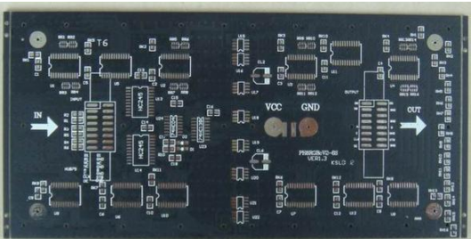
Pcb design
BGA package
The running memory packaged with BGA technology can increase the memory space by two to three tiMES without changing the memory volume. Compared with TSOP, BGA has smaller volume and stronger heat pipe heat dissipation and electrical performance. BGA packaging technology has greatly improved the storage capacity per square inch. Under the same volume, the capacity of the running memory products using BGA packaging technology is only one third of that of TSOP packaging. In addition, compared with the traditional TSOP packaging method, the BGA packaging method has a more rapid and reasonable heat pipe cooling mode.
The I/O terminals of BGA package are distributed under the package in the form of ring or column spot welding array. The advantage of BGA technology is that although the number of I/O pins has increased, the pin spacing has not decreased, but has increased, thus improving the assembly output. Although its power is increased, BGA can be welded by controllable collapse chip method, which can improve its electrothermal performance. The thickness and net weight are lower than the previous packaging technology; The parasitic parameters are reduced, the delay time of data signal transmission is small, and the application frequency is further improved; The assembly can be welded by coplanar electric welding with high reliability.
TinyBGA package
When it comes to BGA packaging, we must mention Kingmax's patent TinyBGA technology. The full English name of TinyBGA is "TinyBallGrid", which belongs to a branch of BGA packaging technology and was successfully developed and designed by Kingmax in August 1999. The ratio of the total chip area to the total package area is not less than 1:1.14, which can increase the memory space by 2-3 times without changing the memory capacity. Compared with TSOP packaged products, it has smaller volume, stronger heat pipe heat dissipation and electrical performance.
Running memory products using TinyBGA packaging technology can only have a volume of 1/3 of TSOP packaging under the same volume condition. The pins of TSOP package running memory are introduced from around the chip, while TinyBGA is introduced from the chip management center. This kind of method reduces the transmission distance of data signal reasonably, and the length of data signal coaxial cable is only 1/4 of that of traditional TSOP technology, so the attenuation coefficient of data signal decreases with it. That not only greatly improves the anti-interference and noise resistance of the chip, but also improves the electrical performance. TinyBGA packaging chip can resist the external frequency up to 300MHz, while traditional TSOP packaging technology can only resist the external frequency up to 150MHz.
The operating memory of TinyBGA package is thinner (package height width ratio is less than 0.8mm), and the reasonable heat pipe heat dissipation relative path from metal material base steel plate to heat pipe radiator is only 0.36mm. As a result, TinyBGA's operating memory has a higher thermal conductivity efficiency, which is very suitable for long-term operating system software and has excellent reliability.
QFP package
QFP is the abbreviation of "QuadFlatPackage", that is, small and medium-sized grid plan package. QFP packaging is often used on independent video cards at the initial stage, but there is little memory of QFP packaging video cards with a speed of more than 4ns. Due to the difficulties of PCB processing technology and performance, TSOP-II and BGA have been gradually replaced at this stage. QFP package contains needle angle around the particles, which is very significant for identification. Four side pin offset flat package. One of the surface mount packages, the pins are led out from the four sides in the form of a gull wing (L).

抖音二维码

Q Q二维码

微信二维码
点击
然后
联系
然后
联系
电话热线
13410863085Q Q

微信

- 邮箱