The Change of Substrate Size in PCB Manufacturing Process
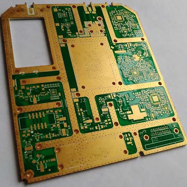
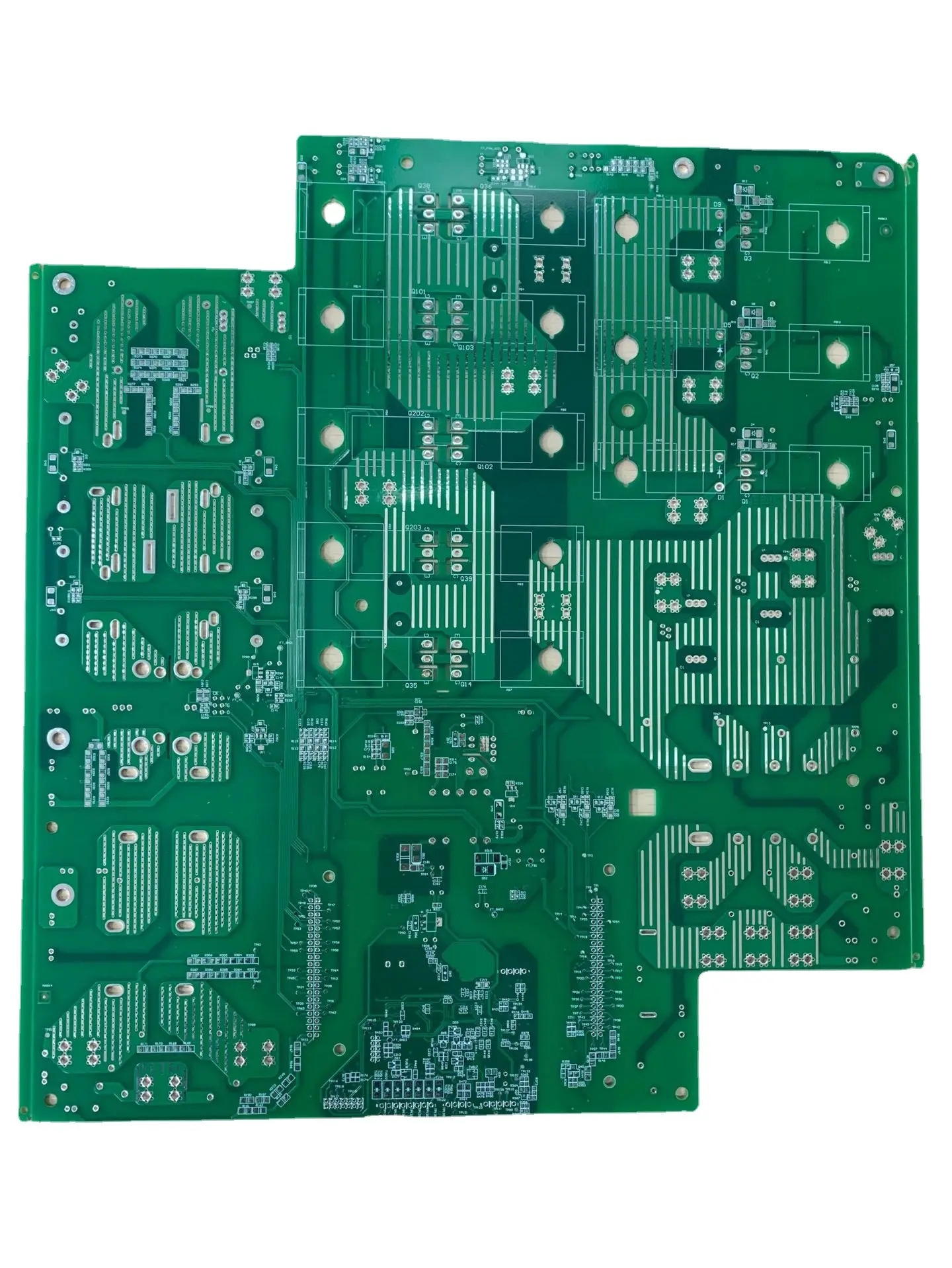
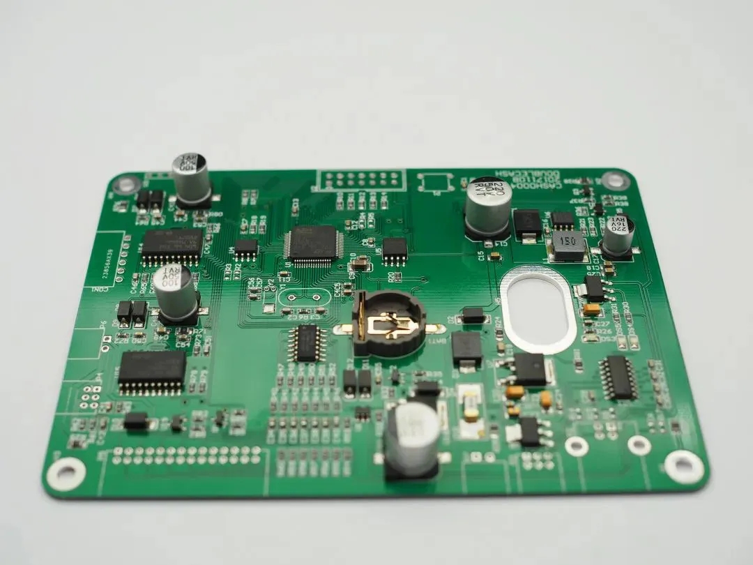
PCB production process, that is, PCB production process. Almost every kind of electronIC equipment, from electronic watches and calculators to computers, communication electronic equipment and military weapon systems, as long as there are integrated circuits and other electronIC components, printed boards are used for their electrical interconnection. In the research process of large-scale electronic products, the most basic success factor is the design, documentation and manufacturing of the product's printed board. The design and manufacturing quality of PCB directly affects the quality and cost of the whole product, and even leads to the success or failure of commercial competition.
printed circuit provides the following functions in electronic equipment:
Provide mechanical support for fixing and assembling various electronic components such as integrated circuits.
To realize wiring and electrical connection or electrical insulation between various electronic components such as integrated circuits.
Provide required electrical characteristics, such as characteristic impedance.
It provides solder resistance graphics for automatic soldering and identification characters and graphics for component insertion, inspection and maintenance.
2、 Some basic terms related to printed boards are as follows:
Printed circuit refers to the conductive pattern made of printed circuit, printed component or combination of both on the insulating substrate according to the predetermined design.
On the insulating substrate, the conductive pattern that provides electrical connection between elements and devices is calLED printed circuit. It does not include printed components.
Printed circuits or the finished boards of printed circuits are called printed circuit boards or printed circuit boards, or printed boards.
reason:
⑴ The difference between longitude and latitude causes the size change of the substrate; When shearing, the fiber direction is not paid attention to, resulting in the residual shear stress in the substrate. Once released, it directly affects the shrinkage of the substrate size.

⑵ The copper foil on the surface of the substrate is etched to limit the change of the substrate, and the size changes when the stress is removed.
(3) When brushing the plate, the pressure is too large, resulting in compressive and tensile stress, which leads to the deformation of the base plate.
(4) The resin in the base plate is not fully cured, resulting in dimensional changes.
(5) Especially, the multilayer boards are stored in poor conditions before lamination, which makes the thin substrate or sEMI solidified sheet hygroscopic, resulting in poor dimensional stability.
(6) Deformation of glass cloth caused by excessive glue flow when multilayer plates are pressed.
resolvent:
⑴ Determine the change rule of the longitude and latitude direction and compensate on the negative film according to the shrinkage rate (this work is carried out before photo drawing). At the same time, the cutting shall be carried out according to the fiber direction, or according to the character signs provided by the manufacturer on the substrate (generally, the vertical direction of the characters is the vertical direction of the substrate).
⑵ The whole board surface shall be evenly distributed as far as possible during circuit design. If it is not possible, a transition section must be left in the space (mainly not affecting the circuit position). This is due to the difference in the density of warp and weft yarns in the glass fabric structure, which leads to the difference in the strength of the plate in the warp and weft directions.
(3) Trial brushing shall be adopted to make the process parameters in the best state, and then rigid plate shall be carried out. For thin base materials, chemical cleaning process or electrolysis process shall be used for cleaning.
(4) Bake. In particular, baking shall be carried out before drilling at 120 ℃ for 4 hours to ensure resin curing and reduce the deformation of substrate size due to the influence of cold and heat.
(5) The substrate with the inner layer oxidized must be baked to remove moisture. The processed substrate shall be stored in a vacuum drying box to avoid moisture absorption again.
(6) Process pressure test shall be carried out, and the process parameters shall be adjusted before pressing. At the same time, according to the characteristics of the prepreg, the appropriate amount of glue flow can be selected.
PCB manufacturing, PCB design and PCBA processing manufacturers will explain the change of PCB size during PCB manufacturing.
然后
联系
电话热线
13410863085Q Q

微信

- 邮箱


