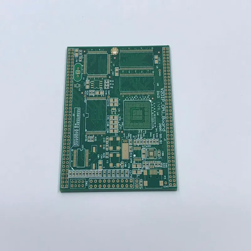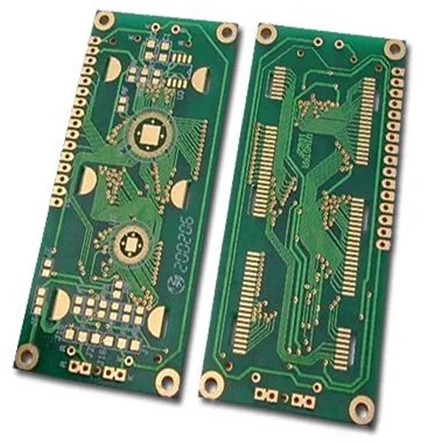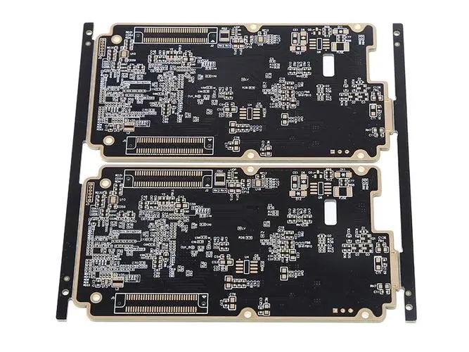
Wiring above 4 layers of high-speed boards and automatIC testing of circuit boards
circuit board manufacturing, circuit board design and PCBA processing manufacturers will explain the wiring of high-speed boards above 4 layers and the field of automatic circuit board testing
Cabling experience of more than 4 layers of high-speed PCB:
1. For wiring above 3 points, try to let the line pass through each point in turn to facilitate testing, and the line length should be as short as possible.
2. Try not to set out wires between pins, especially between and around integrated circuit pins.
3. The lines between different layers should not be parallel as far as possible to avoid the formation of actual capacitance.
4. The wiring shall be straight line or 45 degree broken line to avoid electromagnetic radiation.
5. Ground wire and power wire shall be at least 10-15mil (for logic circuit).
6. Try to connect the grounding wires together to increase the grounding area. The lines shall be as neat as possible.
7. Pay attention to the uniform arrangement of elements for installation, plug-in and welding operations. The text shall be arranged in the current character layer in a reasonable position, and the orientation shall be paid attention to to avoid being blocked, so as to facilitate production.
8. The structure shall be considered for element EMIssion. The positive and negative electrodes of SMD elements shall be MARKed at the end of package to avoid space conflict.
9. At present, the printed circuit board can be used for 4-5mil wiring, but it is usually used for 6mil line width, 8mil line spacing, and 12/20mil bonding pad. The wiring shall consider the influence of the injected current, etc.
10. The components of the function block should be placed together as much as possible, and the components near the LCD such as zebra stripes should not be too close.

11. The vias shall be coated with green oil (set to a negative value).
12. It is better not to place pads, too empty, etc. under the battery holder, and the PAD and VIL dimensions are reasonable.
13. After wiring, carefully check whether each connection line (including NETLABLE) is really connected (lighting method can be used).
14. The oscillating circuit components shall be as close to the IC as possible, and the oscillating circuit shall be as far away from the antenna and other vulnerable areas as possible. The grounding pad shall be placed under the crystal oscillator.
15. Various methods, such as reinforcement and hollow element placement, shall be considered to avoid excessive radiation sources.
PCB boards are widely used in the field of PCB automatic testing
PCB board learned to establish relevant application software on PCB board, and adopted the idea of virtual instrument, that is, to realize various functions of traditional instruments through software, including oscilloscope, signal generator, and various mathematical processing of collected data. During the test, digital signals are given through the test software.
The test system of PCB board will have a new design idea. The design idea of automatic test system based on USB bus and virtual instrument is adopted, which gives full play to the role of the computer. The idea of replacing traditional instruments with computers is tried to reduce the volume of the instrument itself, reduce the development cost, and improve the development efficiency.
After D/A conversion, the analog excitation signal required for the test is applied to the test system, and then sent to the switch matrix by the test circuit through the test bus. The switch matrix is connected to the switch matrix and controlLED by the microprocessor at the same time. The PCB under test is fixed on the needle bed. The excitation signal is applied to the corresponding position of the printed circuit board, and its response is measured by the test circuit. The collected analog quantity is sent to the core control, After A/D conversion, the corresponding digital quantity is obtained, which is fed back by the software on the PCB and processed by the PCB to determine whether the PCB is qualified.
The online testing technology has broken through the previous method of using human eyes to detect circuit boards. The online testing technology has high efficiency, low leak rate, and has realized automation in the detection field. This detection system adopts the idea of combining with virtual instrument, which reduces the hardware design and the cost of the whole system.
The testing system is suitable for the application of SMAll and medium-sized enterprises. It reduces the number of unqualified products entering the next process, thus reducing the rework amount of products, improving the production efficiency, reducing the total cost of manufacturing, and improving the profit of enterprises. It is a widely used testing technology and an efficient, high-speed and high-precision testing method.
At present, PCB boards are used in the field of automatic testing of printed circuit boards in a wide range of tests, including the test of components not installed and the test of components installed. Currently, the commonly used test methods are: on-off test, in circuit test, function test, edge test, optical test and X-ray detection. Online testing is to select an appropriate testing method according to the specific characteristics of PCB board to combine one or more processes, learn from each other and use them comprehensively. circuit board manufacturers, circuit board designers and PCBA manufacturers will explain the wiring and circuit board automatic testing fields above 4 layers of high-speed boards.
然后
联系
电话热线
13410863085Q Q

微信

- 邮箱


